Getting Started Guide: Open FPGA Stack for Intel Agilex 7 FPGAs Targeting the Agilex® 7 FPGA F-Series Development Kit (2x F-Tile)
Last updated: March 26, 2025
1.0 About This Document
The purpose of this document is to help users get started in evaluating the 2024.2-1 version of the PCIe Attach release targeting the F-Series Development Kit. This document will not cover Board Installation Guidelines or OFS Software Installation. Instead it will recommend you use a software installer to allow for fast evaluation. After reviewing this document, a user shall be able to:
- Set up a server environment according to the Best Known Configuration (BKC)
- Load and verify firmware targeting the FIM and AFU regions of the AGFB027R24C2E2VR2 FPGA
- Verify full stack functionality offered by the PCIe Attach OFS solution
- Learn where to find additional information on other PCIe Attach ingredients
1.1 Audience
The information in this document is intended for customers evaluating the PCIe Attach shell targeting the Agilex® 7 FPGA F-Series Development Kit (2x F-Tile). This platform is a Development Kit intended to be used as a starting point for evaluation and development of the Intel Agilex 7 FPGA F-Series with two F-Tiles.
Note: Code command blocks are used throughout the document. Commands that are intended for you to run are preceded with the symbol '$', and comments with '#'. Full command output may not be shown.
1.2 Terminology
Table 1: Terminology
| Term | Abbreviation | Description |
|---|---|---|
| Advanced Error Reporting | AER | The PCIe AER driver is the extended PCI Express error reporting capability providing more robust error reporting. (link) |
| Accelerator Functional Unit | AFU | Hardware Accelerator implemented in FPGA logic which offloads a computational operation for an application from the CPU to improve performance. Note: An AFU region is the part of the design where an AFU may reside. This AFU may or may not be a partial reconfiguration region. |
| Basic Building Block | BBB | Features within an AFU or part of an FPGA interface that can be reused across designs. These building blocks do not have stringent interface requirements like the FIM's AFU and host interface requires. All BBBs must have a (globally unique identifier) GUID. |
| Best Known Configuration | BKC | The software and hardware configuration Intel uses to verify the solution. |
| Board Management Controller | BMC | Supports features such as board power managment, flash management, configuration management, and board telemetry monitoring and protection. The majority of the BMC logic is in a separate component, such as an Intel® Max® 10 or Intel Cyclone® 10 device; a small portion of the BMC known as the PMCI resides in the main Agilex FPGA. |
| Configuration and Status Register | CSR | The generic name for a register space which is accessed in order to interface with the module it resides in (e.g. AFU, BMC, various sub-systems and modules). |
| Data Parallel C++ | DPC++ | DPC++ is Intel’s implementation of the SYCL standard. It supports additional attributes and language extensions which ensure DCP++ (SYCL) is efficiently implanted on Intel hardware. |
| Device Feature List | DFL | The DFL, which is implemented in RTL, consists of a self-describing data structure in PCI BAR space that allows the DFL driver to automatically load the drivers required for a given FPGA configuration. This concept is the foundation for the OFS software framework. (link) |
| FPGA Interface Manager | FIM | Provides platform management, functionality, clocks, resets and standard interfaces to host and AFUs. The FIM resides in the static region of the FPGA and contains the FPGA Management Engine (FME) and I/O ring. |
| FPGA Management Engine | FME | Performs reconfiguration and other FPGA management functions. Each FPGA device only has one FME which is accessed through PF0. |
| Host Exerciser Module | HEM | Host exercisers are used to exercise and characterize the various host-FPGA interactions, including Memory Mapped Input/Output (MMIO), data transfer from host to FPGA, PR, host to FPGA memory, etc. |
| Input/Output Control | IOCTL | System calls used to manipulate underlying device parameters of special files. |
| Intel Virtualization Technology for Directed I/O | Intel VT-d | Extension of the VT-x and VT-I processor virtualization technologies which adds new support for I/O device virtualization. |
| Joint Test Action Group | JTAG | Refers to the IEEE 1149.1 JTAG standard; Another FPGA configuration methodology. |
| Memory Mapped Input/Output | MMIO | The memory space users may map and access both control registers and system memory buffers with accelerators. |
| oneAPI Accelerator Support Package | oneAPI-asp | A collection of hardware and software components that enable oneAPI kernel to communicate with oneAPI runtime and OFS shell components. oneAPI ASP hardware components and oneAPI kernel form the AFU region of a oneAPI system in OFS. |
| Open FPGA Stack | OFS | OFS is a software and hardware infrastructure providing an efficient approach to develop a custom FPGA-based platform or workload using an Intel, 3rd party, or custom board. |
| Open Programmable Acceleration Engine Software Development Kit | OPAE SDK | The OPAE SDK is a software framework for managing and accessing programmable accelerators (FPGAs). It consists of a collection of libraries and tools to facilitate the development of software applications and accelerators. The OPAE SDK resides exclusively in user-space. |
| Platform Interface Manager | PIM | An interface manager that comprises two components: a configurable platform specific interface for board developers and a collection of shims that AFU developers can use to handle clock crossing, response sorting, buffering and different protocols. |
| Platform Management Controller Interface | PMCI | The portion of the BMC that resides in the Agilex FPGA and allows the FPGA to communicate with the primary BMC component on the board. |
| Partial Reconfiguration | PR | The ability to dynamically reconfigure a portion of an FPGA while the remaining FPGA design continues to function. For OFS designs, the PR region is referred to as the pr_slot. |
| Port | N/A | When used in the context of the fpgainfo port command it represents the interfaces between the static FPGA fabric and the PR region containing the AFU. |
| Remote System Update | RSU | The process by which the host can remotely update images stored in flash through PCIe. This is done with the OPAE software command "fpgasupdate". |
| Secure Device Manager | SDM | The SDM is the point of entry to the FPGA for JTAG commands and interfaces, as well as for device configuration data (from flash, SD card, or through PCI Express* hard IP). |
| Static Region | SR | The portion of the FPGA design that cannot be dynamically reconfigured during run-time. |
| Single-Root Input-Output Virtualization | SR-IOV | Allows the isolation of PCI Express resources for manageability and performance. |
| SYCL | SYCL | SYCL (pronounced "sickle") is a royalty-free, cross-platform abstraction layer that enables code for heterogeneous and offload processors to be written using modern ISO C++ (at least C++ 17). It provides several features that make it well-suited for programming heterogeneous systems, allowing the same code to be used for CPUs, GPUs, FPGAs or any other hardware accelerator. SYCL was developed by the Khronos Group, a non-profit organization that develops open standards (including OpenCL) for graphics, compute, vision, and multimedia. SYCL is being used by a growing number of developers in a variety of industries, including automotive, aerospace, and consumer electronics. |
| Test Bench | TB | Testbench or Verification Environment is used to check the functional correctness of the Design Under Test (DUT) by generating and driving a predefined input sequence to a design, capturing the design output and comparing with-respect-to expected output. |
| Universal Verification Methodology | UVM | A modular, reusable, and scalable testbench structure via an API framework. In the context of OFS, the UVM enviroment provides a system level simulation environment for your design. |
| Virtual Function Input/Output | VFIO | An Input-Output Memory Management Unit (IOMMU)/device agnostic framework for exposing direct device access to userspace. (link) |
1.3 References and Versions
Table 2: Software and Component Version Summary for OFS PCIe Attach targeting the F-Series Development Kit
The OFS 2024.2-1 PCIe Attach release targeting the F-Series Development Kit is built upon tightly coupled software and Operating System version(s). The repositories listed below are used to manually build the Shell and the AFU portion of any potential workloads. Use this section as a general reference for the versions which compose this release. Specific instructions on building the FIM or AFU are discussed in their respective documents, but are shown here for the sake of completion.
| Component | Version | Download Link |
|---|---|---|
| Quartus | Quartus Prime Pro Version 24.1 | https://www.intel.com/content/www/us/en/software-kit/794624/intel-quartus-prime-pro-edition-design-software-version-24-1-for-linux.html, patches: 0.18, 0.26 |
| Host Operating System | RedHat® Enterprise Linux® (RHEL) 8.10 | https://access.redhat.com/downloads/content/479/ver=/rhel---8/8.10/x86_64/product-software |
| OneAPI-ASP | ofs-2024.2-2 | https://github.com/OFS/oneapi-asp/releases/tag/ofs-2024.2-1, patches: 0.02 |
| OFS Platform AFU BBB | ofs-2024.2-1 | https://github.com/OFS/ofs-platform-afu-bbb/releases/tag/ofs-2024.2-1 |
| OFS FIM Common Resources | 2024.2-1 | https://github.com/OFS/ofs-fim-common/releases/tag/ofs-2024.2-1 |
| AFU Examples | tag: ofs-2024.2-1 | https://github.com/OFS/examples-afu/releases/tag/ofs-2024.2-1 |
| OPAE-SIM | tag: 2.13.0-2 | https://github.com/OPAE/opae-sim |
| OFS SW Installer | OFS 2024.2-1 Release Page |
Table 3: Hardware BKC for OFS PCIe Attach targeting the F-Series Development Kit
The following table highlights the hardware which composes the Best Known Configuration (BKC) for the OFS 2024.2-1 PCIe Attach release targeting F-Series Development Kit.
Note: The Dell R750 server product line is known not to work with this release.
| Component | Link |
|---|---|
| Agilex® 7 FPGA F-Series Development Kit (2x F-Tile) | https://www.intel.com/content/www/us/en/products/details/fpga/development-kits/agilex/agf027-and-agf023.html |
| Intel FPGA Download Cable II | https://www.intel.com/content/www/us/en/products/sku/215664/intel-fpga-download-cable-ii/specifications.html |
| SuperMicro SYS-220HE-FTNR | https://www.supermicro.com/en/products/system/hyper/2u/sys-220he-ftnr |
1.4 Reference Documents
Documentation is collected on https://ofs.github.io/ofs-2024.1-1/.
2.0 OFS Stack Architecture Overview for Reference Platform
2.1 Hardware Components
The OFS hardware architecture decomposes all designs into a standard set of modules, interfaces, and capabilities. Although the OFS infrastructure provides a standard set of functionality and capability, the user is responsible for making the customizations to their specific design in compliance with the specifications outlined in the Shell Technical Reference Manual: OFS for Agilex® 7 PCIe Attach FPGAs.
OFS is a hardware and software infrastructure that provides an efficient approach to developing a customer FPGA-based platform or workload using an Intel, 3rd party, or custom board.
2.1.1 FPGA Interface Manager
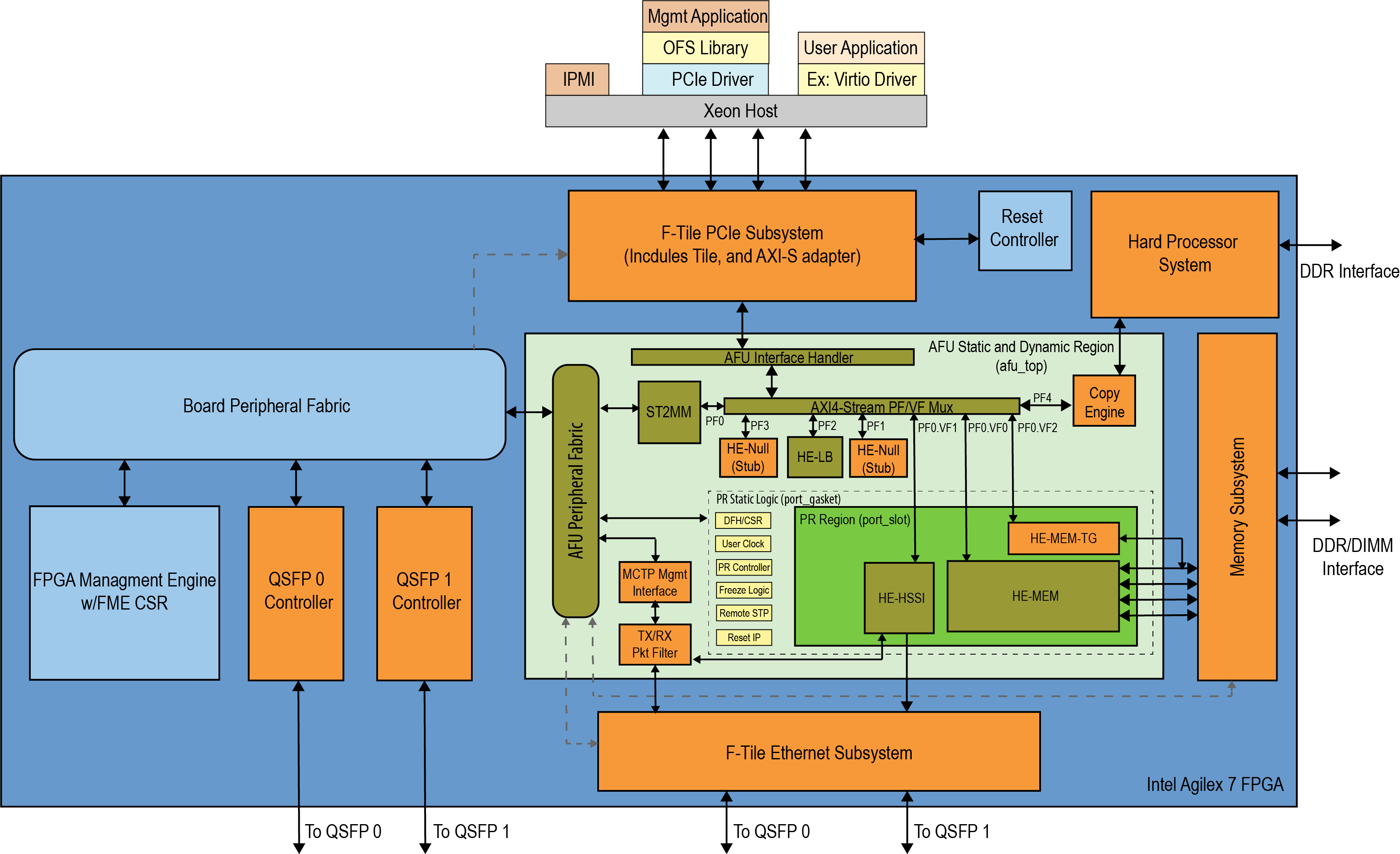
The FPGA Interface Manager (FIM), or shell of the FPGA provides platform management functionality, clocks, resets, and interface access to the host and peripheral features on the acceleration platform. The OFS architecture for Intel Agilex 7 FPGA provides modularity, configurability, and scalability. The primary components of the FPGA Interface Manager or shell of the reference design are:
- PCIe Subsystem - a hierarchical design that targets the P-tile PCIe hard IP and is configured to support Gen4 speeds and Arm AXI4-Stream Data Mover functional mode.
- Ethernet Subsystem - provides portability to different Ethernet configurations across platforms and generations and reusability of the hardware framework and software stack.
- Memory Subsystem - composed of 5 DDR4 channels; two HPS DDR4 banks, x40 (x32 Data and x8 ECC), 1200 MHz, 1GB each, and four Fabric DDR4 banks, x32 (no ECC), 1200 MHz, 4GB
- Hard Processor System - 64-bit quad core ARM® Cortex*-A53 MPCore with integrated peripherals.
- Reset Controller
- FPGA Management Engine - Provides a way to manage the platform and enable acceleration functions on the platform.
- AFU Peripheral Fabric for AFU accesses to other interface peripherals
- Board Peripheral Fabric for master to slave CSR accesses from Host or AFU
- Platform Management Controller Interface (PMCI) to the board management controller
The FPGA Management Engine (FME) provides management features for the platform and the loading/unloading of accelerators through partial reconfiguration. Each feature of the FME exposes itself to the kernel-level OFS drivers on the host through a Device Feature Header (DFH) register that is placed at the beginning of Control Status Register (CSR) space. Only one PCIe link can access the FME register space in a multi-host channel design architecture at a time.
Note: For more information on the FIM and its external connections, refer to the Shell Technical Reference Manual: OFS for Agilex® 7 PCIe Attach FPGAs.
2.1.2 AFU
An AFU is an acceleration workload that interfaces to the FIM. The AFU boundary in this reference design comprises both static and partial reconfiguration (PR) regions. You can decide how you want to partition these two areas or if you want your AFU region to only be a partial reconfiguration region. A port gasket within the design provides all the PR specific modules and logic required to support partial reconfiguration. Only one partial reconfiguration region is supported in this design.
Like the FME, the port gasket exposes its capability to the host software driver through a DFH register placed at the beginning of the port gasket CSR space. In addition, only one PCIe link can access the port register space.
You can compile your design in one of the following ways:
- Your entire AFU resides in a partial reconfiguration region of the FPGA.
- The AFU is part of the static region and is compiled as a flat design.
- Your AFU contains both static and PR regions.
In this design, the AFU region is comprised of:
- AFU Interface handler to verify transactions coming from AFU region.
- PF/VF Mux to route transactions to and from corresponding AFU components: ST2MM module, Virtio LB stub, PCIe loopback host exerciser (HE-LB), HSSI host exerciser (HE-HSSI), Memory Host Exerciser (HE-MEM), Traffic Generator to memory (HE-MEM-TG), Port Gasket (PRG) and HPS Copy Engine.
- AXI4 Streaming to Memory Map (ST2MM) Module that routes MMIO CSR accesses to FME and board peripherals.
- Host exercisers to test PCIe, memory and HSSI interfaces (these can be removed from the AFU region after your FIM design is complete to provide more resource area for workloads)
- Basic HPS Copy Engine to copy second-stage bootloader and Linux OS image from Host DDR to HPS DDR.
- Port gasket and partial reconfiguration support.
- Component for handling PLDM over MCTP over PCIe Vendor Defined Messages (VDM)
The AFU has the option to consume native packets from the host or interface channels or to instantiate a shim provided by the Platform Interface Manager (PIM) to translate between protocols.
Note: For more information on the Platform Interface Manager and AFU development and testing, refer to the Workload Developer Guide: OFS for Agilex® 7 PCIe Attach FPGAs.
3.0 Board Installation and Server Requirements
Instructions detailing the board installation guidelines for an F-Tile Dev Kit including server BIOS settings and regulatory information can be found in the Board Installation Guidelines: Intel Agilex® 7 FPGA F-Series Development Kit (2x F-Tile) and Intel Agilex® 7 FPGA I-Series Development Kit (2x R-Tile and 1xF-Tile). This document also covers the installation of a JTAG cable, which is required for shell programming.
4.0 F-Series Development Kit JTAG Driver Setup
A specific JTAG driver needs to be installed on the host OS. Follow the instructions under the driver setup for Red Hat 5+ on Intel® FPGA Download Cable (formerly USB-Blaster) Driver for Linux*.
View the JTAG Chain after installing the proper driver and Quartus Programmer.
cd ~/intelFPGA_pro/quartus/bin
./jtagconfig -D
1) AGI FPGA Development Kit [1-13]
   (JTAG Server Version 23.3.0 Build 104 09/20/2023 SC Pro Edition)
  034BB0DD   AGIB027R29A(.|R2|R3)/.. (IR=10)
  020D10DD   VTAP10 (IR=10)
    Design hash    27AA3E0B7CE0A5B9F366
    + Node 08586E00  (110:11) #0
    + Node 0C006E00  JTAG UART #0
    + Node 19104600  Nios II #0
    + Node 30006E02  Signal Tap #2
    + Node 30006E01  Signal Tap #1
    + Node 30006E00  Signal Tap #0

  Captured DR after reset = (0069761BB020D10DD) [65]
  Captured IR after reset = (000D55) [21]
  Captured Bypass after reset = (2) [3]
  Captured Bypass chain = (0) [3]
  JTAG clock speed auto-adjustment is enabled. To disable, set JtagClockAutoAdjust parameter to 0
  JTAG clock speed 24 MHz
4.1 Upgrading the F-Series Development Kit FIM via JTAG
Intel provides a pre-built FIM that can be used out-of-box for platform bring-up. This shell design is available on the OFS 2024.2-1 Release Page. After programming the shell and installing both the OPAE SDK and Backport Linux DFL kernel drivers as shown in the Software Installation Guide: Open FPGA Stack for PCIe Attach, you can confirm the correct FIM has been configured by checking the output of fpgainfo fme against the following table:
Table 4: FIM Version
| Identifier | Value |
|---|---|
| Pr Interface ID | 98ed516f-d24d-5b71-ae12-e78cd641e4be |
| Bitstream ID | 360571656856467345 |
You will need to download and unpack the artifact images for this release before upgrading your device. You also need to set up the F-Series Development Kit as outlined in the Board Installation Guidelines: Intel Agilex® 7 FPGA F-Series Development Kit (2x F-Tile) and Intel Agilex® 7 FPGA I-Series Development Kit (2x R-Tile and 1xF-Tile). The file ofs_top_hps.sof is the base OFS FIM file. This file is loaded into the FPGA using the development kit built in USB Blaster. Please be aware this FPGA is not loaded into non-volatile storage. If the server is power cycled you will need to reload the FPGA .sof file.
wget https://github.com/OFS/ofs-agx7-pcie-attach/releases/download/ofs-2024.2-1/fseries-dk-images_ofs-2024-2-1.tar.gz
tar xf fseries-dk-images.tar.gz
cd fseries-dk-images/
This walkthrough describes the steps to program the Agilex FPGA on the Agilex® 7 FPGA F-Series Development Kit (2x F-Tile) with a SOF image via JTAG.
Pre-Requisites:
- This walkthrough requires an OFS Agilex PCIe Attach deployment environment. Refer to the Getting Started Guide: OFS for Agilex® 7 PCIe Attach FPGAs (F-Series Development Kit (2xF-Tile)))) for instructions on setting up a deployment environment.
- This walkthrough requires a
SOFimage which will be programmed to the Agilex FPGA. Refer to the [Walkthrough: Compile OFS FIM] Section for step-by-step instructions for generating aSOFimage.
- This walkthrough requires a JTAG connection to the fseries-dk. Refer to the [Walkthrough: Set up JTAG] section for step-by-step instructions.
- This walkthrough requires a Full Quartus Installation or Standalone Quartus Prime Programmer & Tools running on the machine where the Agilex® 7 FPGA F-Series Development Kit (2x F-Tile) is connected via JTAG.
Steps:
-
Start in your deployment environment.
-
If the card is already programmed with an OFS enabled design, determine the PCIe B:D.F of the card using OPAE command
fpgainfo fme. In this example, the PCIe B:D.F isB1:00.0.Example output:
Intel Acceleration Development Platform N6001
board_n6000.c:306:read_bmcfw_version() **ERROR** : Failed to get read object
board_n6000.c:482:print_board_info() **ERROR** : Failed to read bmc version
board_n6000.c:332:read_max10fw_version() **ERROR** : Failed to get read object
board_n6000.c:488:print_board_info() **ERROR** : Failed to read max10 version
Board Management Controller NIOS FW version:
Board Management Controller Build version:
//****** FME ******//
Interface                        : DFL
Object Id                        : 0xEF00001
PCIe s:b:d.f                     : 0000:B1:00.0
Vendor Id                        : 0x8086
Device Id                        : 0xBCCE
SubVendor Id                     : 0x8086
SubDevice Id                     : 0x1771
Socket Id                        : 0x00
Ports Num                        : 01
Bitstream Id                     : 0x5010202A8769764
Bitstream Version                : 5.0.1
Pr Interface Id                  : b541eb7c-3c7e-5678-a660-a54f71594b34
Boot Page                        : N/A
Note: The errors related to the BMC are the result of the OFS BMC not being present on the fseries-dk design. These will be removed in a future release.
-
Remove the card from PCIe prior to programming. This will disable AER for the PCIe root port to prevent a surprise link-down event during programming.
-
Switch to the machine with JTAG connection to the fseries-dk, if different than your deployment machine.
-
Open the Quartus programmer GUI
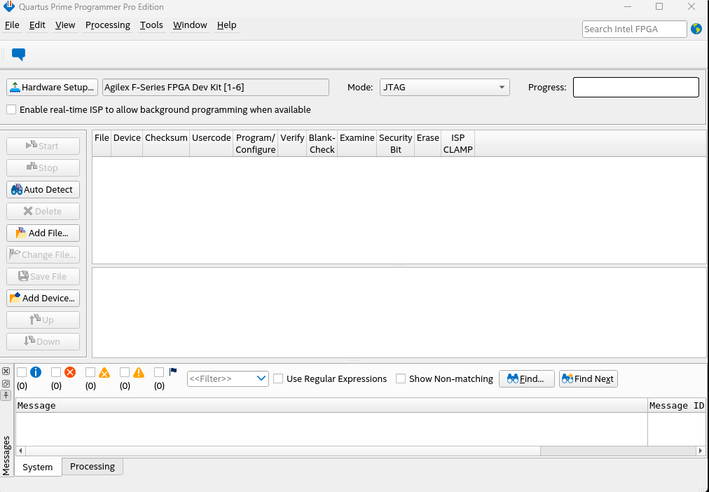
-
Click Hardware Setup to open the Hardware Setup dialog window.
-
In the Currently selected hardware field select the fseries-dk.
-
In the Hardware frequency field enter
16000000Hz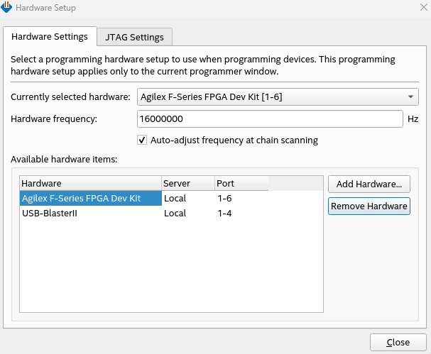
-
Click Close
-
-
In the Quartus Prime Programmer window, click Auto Detect.
-
If prompted, select the AGFB027R24C2E2VR2 device. The JTAG chain should show the device.
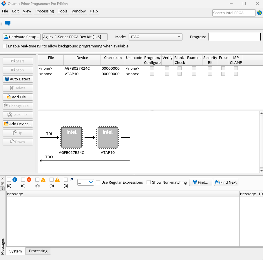
-
Right click the AGFB027R24C2E2VR2 row and selct Change File.
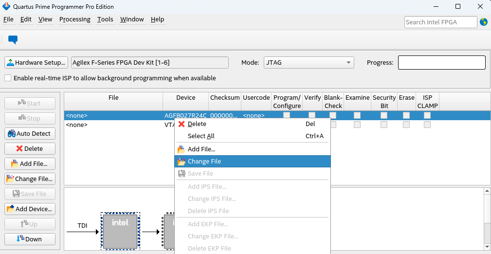
-
In the Select New Programming File window that opens, select
ofs_top_hps.sofand click Open. -
Check the Program/Configure box for the AGFB027R24C2E2VR2 row, then click Start. Wait for the Progress bar to show
100% (Success).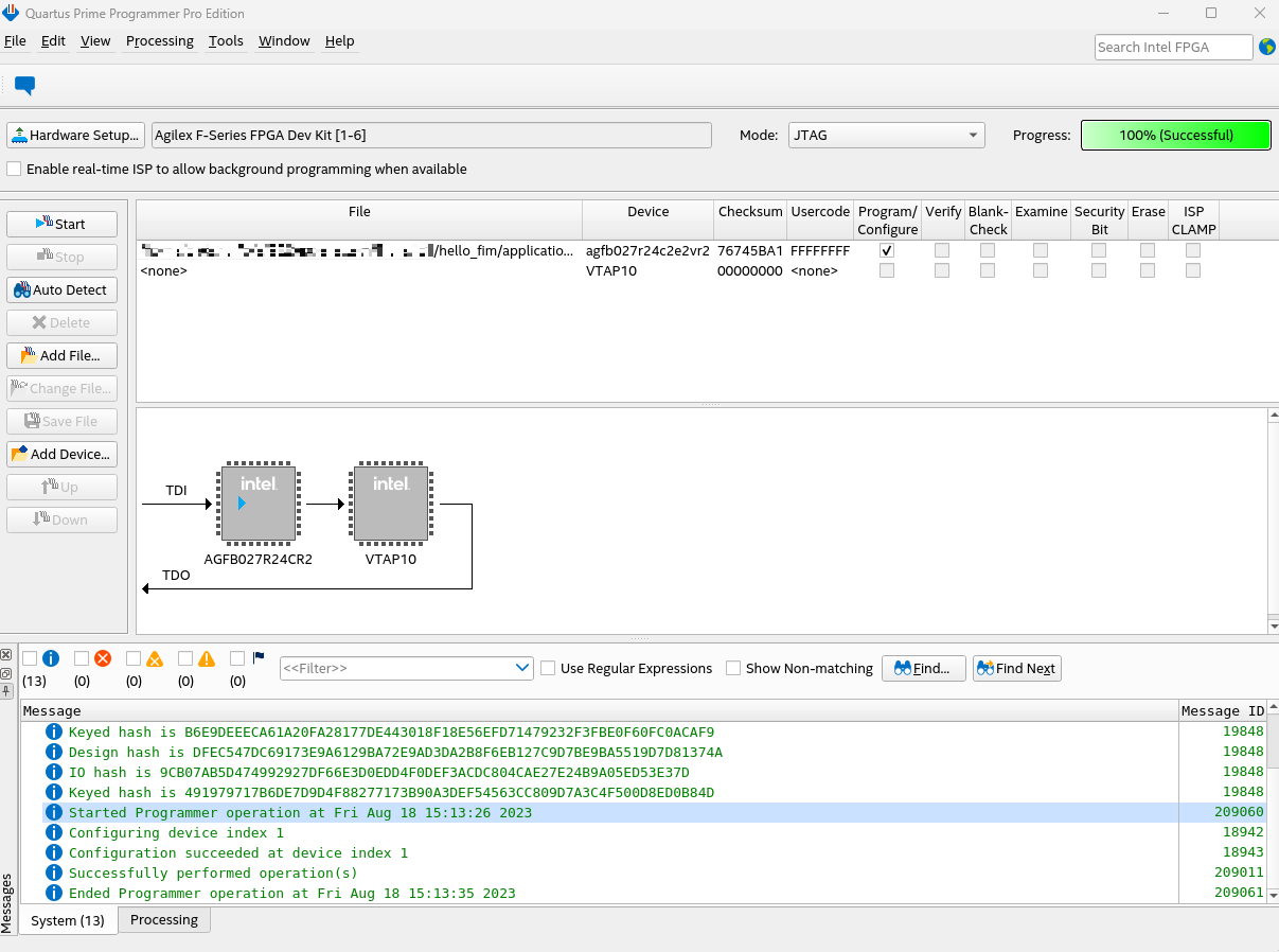
-
Close the Quartus Programmer GUI.
-
Switch to the deployment environment, if different than the JTAG connected machine.
-
Replug the board PCIe
-
Run
fpgainfo fmeto verify communication with the board, and to check the PR Interface ID.Intel Acceleration Development Platform N6001 board_n6000.c:306:read_bmcfw_version() **ERROR** : Failed to get read object board_n6000.c:482:print_board_info() **ERROR** : Failed to read bmc version board_n6000.c:332:read_max10fw_version() **ERROR** : Failed to get read object board_n6000.c:488:print_board_info() **ERROR** : Failed to read max10 version Board Management Controller NIOS FW version: Board Management Controller Build version: //****** FME ******// Interface : DFL Object Id : 0xEF00001 PCIe s:b:d.f : 0000:B1:00.0 Vendor Id : 0x8086 Device Id : 0xBCCE SubVendor Id : 0x8086 SubDevice Id : 0x1771 Socket Id : 0x00 Ports Num : 01 Bitstream Id : 360571656856467345 Bitstream Version : 5.0.1 Pr Interface Id : 98ed516f-d24d-5b71-ae12-e78cd641e4be Boot Page : N/ANote: The errors related to the BMC are the result of the OFS BMC not being present on the fseries-dk design. These will be removed in a future release.
5.0 OFS Software Installation from Script
An overview of the OFS software stack responsibilities and components can be found in the Software Installation Guide: Open FPGA Stack for PCIe Attach. In this document, we will instead use the provided PCIe Attach software installation script to quickly bring up the platform.
Before running the software installer, it is recommended you perform the following steps to lock your OS version to 8.10 and enable related repositories:
subscription-manager release --set=8.10
sudo dnf update
subscription-manager repos --enable codeready-builder-for-rhel-8-x86_64-rpms
sudo dnf install https://dl.fedoraproject.org/pub/epel/epel-release-latest-8.noarch.rpm
Download the OFS PCIe Attach installation script from the OFS 2024.2-1 Release Page. Unpack the files:
wget https://github.com/OFS/ofs-agx7-pcie-attach/releases/download/ofs-2024.2-1/pcieattach_sw_installer_2024.1.zip

unzip pcieattach_sw_installer_2024.1.zip
Executing the script without any input arguments will cause it to set up your local environment and will pull down and install pre-built OFS software artifacts. You can explore its other functionality as looking at the help output ofs_sw_install.py -h or though the included README. Execute the script.
You can check that all OPAE packages have been installed and match expectation:
rpm -qa | grep opae
opae-2.13.0-3.el8.x86_64.rpm
opae-debuginfo-2.13.0-3.el8.x86_64.rpm
opae-debugsource-2.13.0-3.el8.x86_64.rpm
opae-devel-2.13.0-3.el8.x86_64.rpm
opae-devel-debuginfo-2.13.0-3.el8.x86_64.rpm
opae-extra-tools-2.13.0-3.el8.x86_64.rpm
opae-extra-tools-debuginfo-2.13.0-3.el8.x86_64.rpm
To verify the Backport DFL kernel and driver stack have been installed, perform a warm reboot and check with uname.
Note: Your kernel version and tags may differ from the below, depending on script arguments
You can also check the contents of /usr/lib/modules/<kernel name>/kernel/drivers, or run modinfo <driver name>. Below is a list of the drivers which are loaded as a part of the F Tile Dev Kit Shell design:
lsmod | grep dfl

qsfp_mem_dfl           16384  0
qsfp_mem_core          20480  1 qsfp_mem_dfl
uio_dfl                20480  0
uio                    28672  1 uio_dfl
dfl_fme_mgr            20480  1
dfl_emif               16384  0
dfl_fme_region         20480  0
dfl_fme_br             16384  0
dfl_afu                36864  0
dfl_fme                49152  0
dfl_pci                20480  0
dfl                    40960  7 dfl_pci,uio_dfl,dfl_fme,dfl_fme_br,qsfp_mem_dfl,dfl_afu,dfl_emif
fpga_region            20480  3 dfl_fme_region,dfl_fme,dfl
fpga_bridge            24576  4 dfl_fme_region,fpga_region,dfl_fme,dfl_fme_br
fpga_mgr               24576  4 dfl_fme_region,fpga_region,dfl_fme_mgr,dfl_fme
5.1 Memlock limit
Depending on the requirements of any loaded applications, you may also want to increase the maximum amount of memory a user process is allowed to lock. The exact way to do this depends on your Linux distribution.
You can check the current memlock limit using:
A way to permanently remove the limit for locked memory for a regular user is to add the following lines to your /etc/security/limits.conf:
This removes the limit on locked memory for user user1. To remove it for all users, you can replace user1 with *:
Note that settings in the /etc/security/limits.conf file don't apply to services. To increase the locked memory limit for a service you need to modify the application's systemd service file and add the line:
6.0 OPAE Tools Overview
The following section offers a brief introduction including expected output values for the utilities included with OPAE. A full explanation of each command with a description of its syntax is available in the opae-sdk GitHub repo.
A list of all tools included in the OPAE SDK release can be found on the OPAE FPGA Tools tab of ofs.github.io.
6.0.1 Board Management with fpgainfo
The fpgainfo utility displays FPGA information derived from sysfs files.
Displays FPGA information derived from sysfs files. The command argument is one of the following: errors, power, temp, port, fme, bmc, phy or mac, security. Some commands may also have other arguments or options that control their behavior.
For systems with multiple FPGA devices, you can specify the BDF to limit the output to the FPGA resource with the corresponding PCIe configuration. If not specified, information displays for all resources for the given command.
Note: Your Bitstream ID and PR Interface Id may not match the below examples.
The following examples walk through sample outputs generated by fpgainfo. As the F-Series Development Kit does not contain a traditional BMC as used by other OFS products, those lines in fpgainfo's output will not return valid objects. The subcommand fpgainfo bmc will likewise fail to report telemetry data.
Intel Acceleration JTAG PCI Development Kit
//****** FME ******//
Interface                        : DFL
Object Id                        : 0xEF00001
PCIe s:b:d.f                     : 0000:B1:00.0
Vendor Id                        : 0x8086
Device Id                        : 0xBCCE
SubVendor Id                     : 0x8086
SubDevice Id                     : 0x1771
Socket Id                        : 0x00
Ports Num                        : 01
Bitstream Id                     : 0x501020241BF165B
Bitstream Version                : 5.0.1
Pr Interface Id                  : b4eda250-cdb7-5891-a06e-13d28d09bc32
Boot Page                        : N/A
6.0.2 Updating with fpgasupdate
The fpgasupdate tool is used to program AFU workloads into an open slot in a FIM. The fpgasupdate tool only accepts images that have been formatted using PACsign.
As the F-Series Development Kit does not contain a traditional BMC, you do not have access to a factory, user1, and user2 programmed image for both the FIM and BMC FW and RTL. Only the programming of a GBS workload is supported for this release.
The process of programming a SOF with a new FIM version is shown in section 4.0 Upgrading the F-Series Development Kit FIM via JTAG
sudo fpgasupdate ofs_pr_afu.gbs   <PCI ADDRESS>
[2022-04-14 16:42:31.58] [WARNING ] Update starting. Please do not interrupt.
[2022-04-14 16:42:31.58] [INFO    ] updating from file ofs_pr_afu.gbs with size 19928064
[2022-04-14 16:42:31.60] [INFO    ] waiting for idle
[2022-04-14 16:42:31.60] [INFO    ] preparing image file
[2022-04-14 16:42:38.61] [INFO    ] writing image file
(100%) [████████████████████] [19928064/19928064 bytes][Elapsed Time: 0:00:16.01]
[2022-04-14 16:42:54.63] [INFO    ] programming image file
(100%) [████████████████████][Elapsed Time: 0:06:16.40]
[2022-04-14 16:49:11.03] [INFO    ] update of 0000:b1:00.0 complete
[2022-04-14 16:49:11.03] [INFO    ] Secure update OK
[2022-04-14 16:49:11.03] [INFO    ] Total time: 0:06:39.45
6.0.3 Verify FME Interrupts with hello_events
The hello_events utility is used to verify FME interrupts. This tool injects FME errors and waits for error interrupts, then clears the errors.
Sample output from sudo hello_events.
sudo hello_events
Waiting for interrupts now...
injecting error
FME Interrupt occurred
Successfully tested Register/Unregister for FME events!
clearing error
6.1 Host Exerciser Modules
The reference FIM and unchanged FIM compilations contain Host Exerciser Modules (HEMs). These are used to exercise and characterize the various host-FPGA interactions, including Memory Mapped Input/Output (MMIO), data transfer from host to FPGA, PR, host to FPGA memory, etc. There are three HEMs present in the Intel OFS Reference FIM - HE-LPBK, HE-MEM, and HE-HSSI. These exercisers are tied to three different VFs that must be enabled before they can be used. Execution of these exercisers requires you bind specific VF endpoint to vfio-pci. The host-side software looks for these endpoints to grab the correct FPGA resource.
Refer to the Intel Shell Technical Reference Manual: OFS for Agilex® 7 PCIe Attach FPGAs for a full description of these modules.
Table 5: Module PF/VF Mappings
| Module | PF/VF |
|---|---|
| ST2MM | PF0 |
| HE-MEM | PF0-VF0 |
| HE-HSSI | PF0-VF1 |
| HE-MEM_TG | PF0-VF2 |
| HE-LB Stub | PF1-VF0 |
| HE-LB | PF2 |
| VirtIO LB Stub | PF3 |
| HPS Copy Engine | PF4 |
6.1.1 HE-MEM / HE-LB
The host exerciser used to exercise and characterize the various host-FPGA interactions eg. MMIO, Data transfer from host to FPGA , PR, host to FPGA memory etc. The Host Exerciser Loopback (HE-LBK) AFU can move data between host memory and FPGA.
HE-LBK supports: - Latency (AFU to Host memory read) - MMIO latency (Write+Read) - MMIO BW (64B MMIO writes) - BW (Read/Write, Read only, Wr only)
The Host Exerciser Loopback Memory (HE-MEM) AFU is used to exercise use of FPGA connected DDR, data read from the host is written to DDR, and the same data is read from DDR before sending it back to the host.
HE-LB is responsible for generating traffic with the intention of exercising the path from the AFU to the Host at full bandwidth. HE-MEM is used to exercise use of FPGA connected DDR; data read from the host is written to DDR, and the same data is read from DDR before sending it back to the host. HE-MEM uses external DDR memory (i.e. EMIF) to store data. It has a customized version of the AVMM interface to communicate with the EMIF memory controller. Both exercisers rely on the user-space tool host_exerciser. When using the F-Series Development Kit SmartNIC Platform, optimal performance requires the exercisers be run at 400 MHz.
Execution of these exercisers requires you to bind specific VF endpoint to vfio-pci. The following commands will bind the correct endpoint for a device with B/D/F 0000:b1:00.0 and run through a basic loopback test.
Note: While running the opae.io init command listed below, the command has failed if no output is present after completion. Double check that Intel VT-D and IOMMU have been enabled in the kernel as discussed in section 3.0 OFS DFL Kernel Drivers.
$ sudo pci_device  0000:b1:00.0 vf 3

$ sudo opae.io init -d 0000:b1:00.2 user:user
Unbinding (0x8086,0xbcce) at 0000:b1:00.2 from dfl-pci
Binding (0x8086,0xbcce) at 0000:b1:00.2 to vfio-pci
iommu group for (0x8086,0xbcce) at 0000:b1:00.2 is 188
Assigning /dev/vfio/188 to user
Changing permissions for /dev/vfio/188 to rw-rw----


$ sudo host_exerciser --clock-mhz 400 lpbk
    starting test run, count of 1
API version: 4
Bus width: 64 bytes
AFU clock from command line: 400 MHz
Allocate SRC Buffer
Allocate DST Buffer
Allocate DSM Buffer
    Host Exerciser Performance Counter:
    Host Exerciser numReads: 1024
    Host Exerciser numWrites: 1025
    Host Exerciser numPendReads: 0
    Host Exerciser numPendWrites: 0
    Host Exerciser numPendEmifReads: 0
    Host Exerciser numPendEmifWrites: 0
    Number of clocks: 3002
    Total number of Reads sent: 1024
    Total number of Writes sent: 1024
    Bandwidth: 8.732 GB/s
    Test lpbk(1): PASS
The following example will run a loopback throughput test using one cache line per request.
$ sudo pci_device  0000:b1:00.0 vf 3

$ sudo opae.io init -d 0000:b1:00.2 user:user

$ sudo host_exerciser --clock-mhz 400 --mode trput --cls cl_1 lpbk
    starting test run, count of 1
API version: 4
Bus width: 64 bytes
AFU clock from command line: 400 MHz
Allocate SRC Buffer
Allocate DST Buffer
Allocate DSM Buffer
    Host Exerciser Performance Counter:
    Host Exerciser numReads: 512
    Host Exerciser numWrites: 513
    Host Exerciser numPendReads: 0
    Host Exerciser numPendWrites: 0
    Host Exerciser numPendEmifReads: 0
    Host Exerciser numPendEmifWrites: 0
    Number of clocks: 2014
    Total number of Reads sent: 512
    Total number of Writes sent: 512
    Bandwidth: 13.016 GB/s
    Test lpbk(1): PASS
6.1.2 Traffic Generator AFU Test Application
Beginning in OPAE version 2.0.11-1+ the TG AFU has an OPAE application to access & exercise traffic, targeting a specific bank. The supported arguments for test configuration are:
- Number of test loops: --loops
- Number of read transfers per test loop: -r,--read
- Number of write transfers per test loop: -w,--write
- Burst size of each transfer: -b,--bls
- Address stride between each transfer: --stride
- Target memory TG: -m,--mem-channel
Below are some example commands for how to execute the test application. To run the preconfigured write/read traffic test on channel 0:
Target channel 1 with a 1MB single-word write only test for 1000 iterations
Target channel 2 with 4MB write/read test of max burst length for 10 iterations
sudo mem_tg --loops 1000 -r 2000 -w 2000 --stride 2 --bls 2  -m 1 tg_test
[2022-07-15 00:13:16.349] [tg_test] [info] starting test run, count of 1
Memory channel clock frequency unknown. Assuming 300 MHz.
TG PASS
Mem Clock Cycles: 17565035
Write BW: 4.37232 GB/s
Read BW: 4.37232 GB/s
6.1.3 HE-HSSI
HE-HSSI is responsible for handling client-side ethernet traffic. It wraps the 10G and 100G HSSI AFUs and includes a traffic generator and checker. The user-space tool hssi exports a control interface to the HE-HSSI's AFU's packet generator logic.
The hssi application provides a means of interacting with the 10G and with the 100G HSSI AFUs. In both 10G and 100G operating modes, the application initializes the AFU, completes the desired transfer as described by the mode- specific options, and displays the ethernet statistics by invoking ethtool --statistics INTERFACE.
Due to Ethernet differential pair routing on the ES version of the Intel Agilex® 7 F-Series FPGA (Two F-Tiles) Development Kit, some differential pairs were swapped to improve signal routing. To account for the pair swap, there is a requirement to run a script to invert the differential traces. If you run the command “fpgainfo phy B:d.f” when the Ethernet ports are connected to known good sources and observe the following three ports are down as shown below:
$ sudo fpgainfo phy b1:00.0
Intel Acceleration JTAG PCI Development Kit
//****** PHY ******//
Interface                        : DFL
Object Id                        : 0xEF00001
PCIe s:b:d.f                     : 0000:B1:00.0
Vendor Id                        : 0x8086
Device Id                        : 0xBCCE
SubVendor Id                     : 0x8086
SubDevice Id                     : 0x0001
Socket Id                        : 0x00
Ports Num                        : 01
Bitstream Id                     : 0x50102020CB5B309
Bitstream Version                : 5.0.1
Pr Interface Id                  : d0f93544-a487-5a92-8632-d43f27dbccee
QSFP0                            : Connected
QSFP1                            : Not Connected
//****** HSSI information ******//
HSSI version                     : 2.0
Number of ports                  : 8
Port0                            :25GbE        DOWN
Port1                            :25GbE        DOWN
Port2                            :25GbE        DOWN
Port3                            :25GbE        DOWN
Port4                            :25GbE        DOWN
Port5                            :25GbE        DOWN
Port6                            :25GbE        DOWN
Port7                            :25GbE        DOWN
Create the following script called “set_tx_inverse_polarity.sh” to set make Transceiver PAM register settings:
#!/bin/sh

# Port 3
base_addr=$(printf "%08d" "0x500000")
address=`expr $base_addr + 589884`
#address=`expr $base_addr + 589884`
offset=`expr $address/4`

hex_number=$(printf "0x%06x" "$(($offset))")
echo $hex_number
cmd_sts=$(printf "%32x" "$(($offset2))")
csraddr="${hex_number}0500000002"
csraddr1="${hex_number}0600000001"
data=1a040
echo $csraddr
sudo opae.io poke  0x140b0 0x0001a26500000000
sleep 1
sudo opae.io poke  0x140a8 $csraddr
sleep 1
sudo opae.io peek  0x140a8
sleep 1

sudo opae.io poke  0x140b0 0x0001226500000000
sleep 1
sudo opae.io poke  0x140a8 $csraddr
sleep 1
sudo opae.io peek  0x140a8
# Port 6

base_addr=$(printf "%08d" "0xb00000")
address=`expr $base_addr + 589884`
#address=`expr $base_addr + 589884`
offset=`expr $address/4`

hex_number=$(printf "0x%06x" "$(($offset))")
echo $hex_number
cmd_sts=$(printf "%32x" "$(($offset2))")
csraddr="${hex_number}0500000002"
csraddr1="${hex_number}0600000001"
data=1a040
echo $csraddr
sudo opae.io poke  0x140b0 0x0001a16500000000
sleep 1
sudo opae.io poke  0x140a8 $csraddr
sleep 1
sudo opae.io peek  0x140a8
sleep 1

sudo opae.io poke  0x140b0 0x0001216500000000
sleep 1
sudo opae.io poke  0x140a8 $csraddr
sleep 1
sudo opae.io peek  0x140a8
# Port 7

base_addr=$(printf "%08d" "0x1100000")
address=`expr $base_addr + 589884`
#address=`expr $base_addr + 589884`
offset=`expr $address/4`

hex_number=$(printf "0x%06x" "$(($offset))")
echo $hex_number
cmd_sts=$(printf "%32x" "$(($offset2))")
csraddr="${hex_number}0500000002"
csraddr1="${hex_number}0600000001"
data=1a040
echo $csraddr
sudo opae.io poke  0x140b0 0x0001a26500000000
sleep 1
sudo opae.io poke  0x140a8 $csraddr
sleep 1
sudo opae.io peek  0x140a8
sleep 1

sudo opae.io poke  0x140b0 0x0001226500000000
sleep 1
sudo opae.io poke  0x140a8 $csraddr
sleep 1
sudo opae.io peek  0x140a8
The script set_tx_inverse_polarity.sh requires the VFIO driver on PF0 to access the Transceiver registers. You will use the opae.io command prior to running set_tx_inverse_polarity.sh to bind the VFIO driver. Once the script completes, release the VFIO driver with opae.io release.
The listing below shows the script being run:
sudo opae.io init -d 0000:b1:00.0 $USER
Unbinding (0x8086,0xbcce) at 0000:b1:00.0 from dfl-pci
Binding (0x8086,0xbcce) at 0000:b1:00.0 to vfio-pci
iommu group for (0x8086,0xbcce) at 0000:b1:00.0 is 8

sh set_tx_inverse_polarity.sh
0x16400f
0x16400f0500000002
0x16400f0500000006
0x16400f0500000006
0x2e400f
0x2e400f0500000002
0x2e400f0500000006
0x2e400f0500000006
0x46400f
0x46400f0500000002
0x46400f0500000006
0x46400f0500000006

sudo opae.io release -d 0000:b1:00.0
Releasing (0x8086,0xbcce) at 0000:b1:00.0 from vfio-pci
Rebinding (0x8086,0xbcce) at 0000:b1:00.0 to dfl-pci

sudo fpgainfo phy b1:00.0
Intel Acceleration JTAG PCI Development Kit
//****** PHY ******//
Interface                        : DFL
Object Id                        : 0xEF00001
PCIe s:b:d.f                     : 0000:B1:00.0
Vendor Id                        : 0x8086
Device Id                        : 0xBCCE
SubVendor Id                     : 0x8086
SubDevice Id                     : 0x1771
Socket Id                        : 0x00
Ports Num                        : 01
Bitstream Id                     : 0x501020241BF165B
Bitstream Version                : 5.0.1
Pr Interface Id                  : 767712e5-b1d0-5777-aea9-592572a6817f
QSFP0                            : Connected
QSFP1                            : Connected
//****** HSSI information ******//
HSSI version                     : 2.0
Number of ports                  : 8
Port0                            :25GbE        UP
Port1                            :25GbE        UP
Port2                            :25GbE        UP
Port3                            :25GbE        UP
Port4                            :25GbE        UP
Port5                            :25GbE        UP
Port6                            :25GbE        UP
Port7                            :25GbE        UP
The following example walks through the process of binding the VF corresponding with the HE-HSSI exerciser to vfio-pci, sending traffic, and verifying that traffic was received.
Table 6: Accelerator PF/VF and GUID Mappings
| Component | VF | Accelerator GUID |
|---|---|---|
| F Series Dev Kit base PF | XXXX:XX:XX.0 | N/A |
| VirtIO Stub | XXXX:XX:XX.1 | 3e7b60a0-df2d-4850-aa31-f54a3e403501 |
| HE-MEM Stub | XXXX:XX:XX.2 | 56e203e9-864f-49a7-b94b-12284c31e02b |
| Copy Engine | XXXX:XX:XX.4 | 44bfc10d-b42a-44e5-bd42-57dc93ea7f91 |
| HE-MEM | XXXX:XX:XX.5 | 8568ab4e-6ba5-4616-bb65-2a578330a8eb |
| HE-HSSI | XXXX:XX:XX.6 | 823c334c-98bf-11ea-bb37-0242ac130002 |
| MEM-TG | XXXX:XX:XX.7 | 4dadea34-2c78-48cb-a3dc-5b831f5cecbb |
-
Create 3 VFs in the PR region.
-
Verify all 3 VFs were created.
lspci -s b1:00 b1:00.0 Processing accelerators: Intel Corporation Device bcce (rev 01) b1:00.1 Processing accelerators: Intel Corporation Device bcce b1:00.2 Processing accelerators: Intel Corporation Device bcce b1:00.3 Processing accelerators: Red Hat, Inc. Virtio network device b1:00.4 Processing accelerators: Intel Corporation Device bcce b1:00.5 Processing accelerators: Intel Corporation Device bccf b1:00.6 Processing accelerators: Intel Corporation Device bccf b1:00.7 Processing accelerators: Intel Corporation Device bccf -
Bind all the PF/VF endpoints to the
vfio-pcidriver.sudo opae.io init -d 0000:b1:00.1 user:user Unbinding (0x8086,0xbcce) at 0000:b1:00.1 from dfl-pci Binding (0x8086,0xbcce) at 0000:b1:00.1 to vfio-pci iommu group for (0x8086,0xbcce) at 0000:b1:00.1 is 187 Assigning /dev/vfio/187 to user Changing permissions for /dev/vfio/187 to rw-rw---- sudo opae.io init -d 0000:b1:00.2 user:user Unbinding (0x8086,0xbcce) at 0000:b1:00.2 from dfl-pci Binding (0x8086,0xbcce) at 0000:b1:00.2 to vfio-pci iommu group for (0x8086,0xbcce) at 0000:b1:00.2 is 188 Assigning /dev/vfio/188 to user Changing permissions for /dev/vfio/188 to rw-rw---- ... sudo opae.io init -d 0000:b1:00.7 user:user Binding (0x8086,0xbccf) at 0000:b1:00.7 to vfio-pci iommu group for (0x8086,0xbccf) at 0000:b1:00.7 is 319 Assigning /dev/vfio/319 to user Changing permissions for /dev/vfio/319 to rw-rw---- -
Check that the accelerators are present using
fpgainfo. Note your port configuration may differ from the below.sudo fpgainfo port //****** PORT ******// Object Id : 0xEC00000 PCIe s:b:d.f : 0000:B1:00.0 Vendor Id : 0x8086 Device Id : 0xBCCE SubVendor Id : 0x8086 SubDevice Id : 0x1771 Socket Id : 0x00 //****** PORT ******// Object Id : 0xE0B1000000000000 PCIe s:b:d.f : 0000:B1:00.7 Vendor Id : 0x8086 Device Id : 0xBCCF SubVendor Id : 0x8086 SubDevice Id : 0x1771 Socket Id : 0x01 Accelerator GUID : 4dadea34-2c78-48cb-a3dc-5b831f5cecbb //****** PORT ******// Object Id : 0xC0B1000000000000 PCIe s:b:d.f : 0000:B1:00.6 Vendor Id : 0x8086 Device Id : 0xBCCF SubVendor Id : 0x8086 SubDevice Id : 0x1771 Socket Id : 0x01 Accelerator GUID : 823c334c-98bf-11ea-bb37-0242ac130002 //****** PORT ******// Object Id : 0xA0B1000000000000 PCIe s:b:d.f : 0000:B1:00.5 Vendor Id : 0x8086 Device Id : 0xBCCF SubVendor Id : 0x8086 SubDevice Id : 0x1771 Socket Id : 0x01 Accelerator GUID : 8568ab4e-6ba5-4616-bb65-2a578330a8eb //****** PORT ******// Object Id : 0x80B1000000000000 PCIe s:b:d.f : 0000:B1:00.4 Vendor Id : 0x8086 Device Id : 0xBCCE SubVendor Id : 0x8086 SubDevice Id : 0x1771 Socket Id : 0x01 Accelerator GUID : 44bfc10d-b42a-44e5-bd42-57dc93ea7f91 //****** PORT ******// Object Id : 0x40B1000000000000 PCIe s:b:d.f : 0000:B1:00.2 Vendor Id : 0x8086 Device Id : 0xBCCE SubVendor Id : 0x8086 SubDevice Id : 0x1771 Socket Id : 0x01 Accelerator GUID : 56e203e9-864f-49a7-b94b-12284c31e02b //****** PORT ******// Object Id : 0x20B1000000000000 PCIe s:b:d.f : 0000:B1:00.1 Vendor Id : 0x8086 Device Id : 0xBCCE SubVendor Id : 0x8086 SubDevice Id : 0x1771 Socket Id : 0x01 Accelerator GUID : 3e7b60a0-df2d-4850-aa31-f54a3e403501 -
Check Ethernet PHY settings with
fpgainfo.sudo fpgainfo phy -B 0xb1 Intel Acceleration JTAG PCI Development Kit //****** PHY ******// Interface : DFL Object Id : 0xEF00001 PCIe s:b:d.f : 0000:B1:00.0 Vendor Id : 0x8086 Device Id : 0xBCCE SubVendor Id : 0x8086 SubDevice Id : 0x0001 Socket Id : 0x00 Ports Num : 01 Bitstream Id : 0x50102020CB5B309 Bitstream Version : 5.0.1 Pr Interface Id : d0f93544-a487-5a92-8632-d43f27dbccee QSFP0 : Connected QSFP1 : Not Connected //****** HSSI information ******// HSSI version : 2.0 Number of ports : 8 Port0 :25GbE DOWN Port1 :25GbE DOWN Port2 :25GbE DOWN Port3 :25GbE DOWN Port4 :25GbE DOWN Port5 :25GbE DOWN Port6 :25GbE DOWN Port7 :25GbE DOWN -
Set loopback mode.
sudo hssiloopback --loopback enable --pcie-address 0000:b1:00.0 args Namespace(loopback='enable', pcie_address='0000:b1:00.0', port=0) sbdf: 0000:b1:00.0 FPGA dev: {'segment': 0, 'bus': 177, 'dev': 0, 'func': 0, 'path': '/sys/class/fpga_region/region0', 'pcie_address': '0000:b1:00.0'} args.hssi_grps{0: ['dfl_dev.6', ['/sys/bus/pci/devices/0000:b1:00.0/fpga_region/region0/dfl-fme.0/dfl_dev.6/uio/uio0']]} fpga uio dev:dfl_dev.6 --------HSSI INFO START------- DFH :0x3000000010002015 HSSI ID :0x15 DFHv :0.5 guidl :0x99a078ad18418b9d guidh :0x4118a7cbd9db4a9b HSSI version :1.0 Firmware Version :1 HSSI num ports :8 Port0 :25GbE Port1 :25GbE Port2 :25GbE Port3 :25GbE Port4 :25GbE Port5 :25GbE Port6 :25GbE Port7 :25GbE --------HSSI INFO END------- hssi loopback enabled to port0 -
Send traffic through the 10G AFU.
$sudo hssi --pci-address b1:00.6 hssi_10g --num-packets 100
10G loopback test
    Tx/Rx port: 99
    Tx port: 0
    Rx port: 0
    eth_loopback: on
    he_loopback: none
    num_packets: 100
    packet_length: 64
    src_address: 11:22:33:44:55:66
    (bits): 0x665544332211
    dest_address: 77:88:99:aa:bb:cc
    (bits): 0xccbbaa998877
    random_length: fixed
    random_payload: incremental
    rnd_seed0: 5eed0000
    rnd_seed1: 5eed0001
    rnd_seed2: 25eed
    eth:

No eth interface, so not honoring --eth-loopback. Try using the hssiloopback command instead.
0x40000           ETH_AFU_DFH: 0x1000010000001000
0x40008          ETH_AFU_ID_L: 0xbb370242ac130002
0x40010          ETH_AFU_ID_H: 0x823c334c98bf11ea
0x40030      TRAFFIC_CTRL_CMD: 0x0000000000000000
0x40038     TRAFFIC_CTRL_DATA: 0x0000000100000000
0x40040 TRAFFIC_CTRL_PORT_SEL: 0x0000000000000000
0x40048        AFU_SCRATCHPAD: 0x0000000045324511

0x3c00         number_packets: 0x00000064
0x3c01          random_length: 0x00000000
0x3c02         random_payload: 0x00000000
0x3c03                  start: 0x00000000
0x3c04                   stop: 0x00000000
0x3c05           source_addr0: 0x44332211
0x3c06           source_addr1: 0x00006655
0x3c07             dest_addr0: 0xaa998877
0x3c08             dest_addr1: 0x0000ccbb
0x3c09        packet_tx_count: 0x00000064
0x3c0a              rnd_seed0: 0x5eed0000
0x3c0b              rnd_seed1: 0x5eed0001
0x3c0c              rnd_seed2: 0x00025eed
0x3c0d             pkt_length: 0x00000040
0x3cf4          tx_sta_tstamp: 0x02ab5f6d
0x3cf5          tx_end_tstamp: 0x02ab63dd
0x3d00                num_pkt: 0xffffffff
0x3d01               pkt_good: 0x00000064
0x3d02                pkt_bad: 0x00000000
0x3d07            avst_rx_err: 0x00000000
0x3d0b          rx_sta_tstamp: 0x02ab6058
0x3d0c          rx_end_tstamp: 0x02ab64dc
0x3e00               mac_loop: 0x00000000

HSSI performance:
        Selected clock frequency : 402.832 MHz
        Latency minimum : 583.37 ns
        Latency maximum : 633.018 ns
        Achieved Tx throughput : 15.8863 GB/s
        Achieved Rx throughput : 15.6115 GB/s
The hssi_loopback utility works in conjunction with a packet generator accelerator function unit (AFU) to test high-speed serial interface (HSSI) cards. hssi_loopback tests both external and internal loopbacks.
The hssistats tool provides the MAC statistics.