Getting Started Guide: Open FPGA Stack for Intel® Agilex FPGAs Targeting the Intel® FPGA SmartNIC N6001-PL
1.0 Introduction
1.1 About This Document
The purpose of this document is to help users get started in evaluating the 2023.1 version of the Open FPGA Stack (OFS) for the Intel Agilex FPGA targeting the Intel N6001-PL FPGA SmartNIC Platform. After reviewing the document a user shall be able to:
- Set up their server environment according to the Best Known Configuration (BKC)
- Build and install the OFS Linux Kernel drivers
- Build and install the Open Programmable Acceleration Engine Software Development Kit (OPAE SDK) software on top of the OFS Linux kernel drivers
- Load and Verify the Firmware and FIM versions loaded on their boards
- Verify the full stack functionality offered by the OFS solution
- Know where to find additional information on other OFS ingredients
The following flow charts show a high level overview of the initial bring up process, split into three sequential diagrams. Detailed instructions for each installation process are shown in their respective sections.
Diagram 1: Installing the OPAE SDK
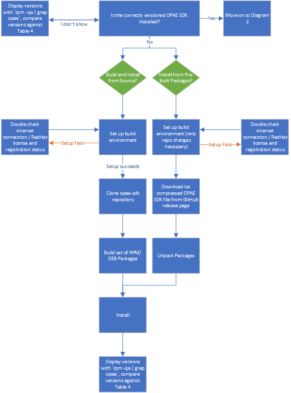
Diagram 2: Installing the Linux DFL Drivers
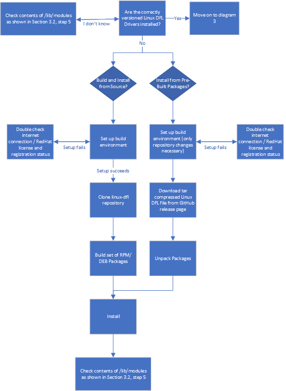
Diagram 3: Bringing up the Intel® FPGA SmartNIC N6001-PL
1.2 Terminology
Table 1: Glossary
| Term | Abbreviation | Description |
|---|---|---|
| Advanced Error Reporting | AER | The PCIe AER driver is the extended PCI Express error reporting capability providing more robust error reporting. (link) |
| Accelerator Functional Unit | AFU | Hardware Accelerator implemented in FPGA logic which offloads a computational operation for an application from the CPU to improve performance. Note: An AFU region is the part of the design where an AFU may reside. This AFU may or may not be a partial reconfiguration region. |
| Basic Building Block | BBB | Features within an AFU or part of an FPGA interface that can be reused across designs. These building blocks do not have stringent interface requirements like the FIM's AFU and host interface requires. All BBBs must have a (globally unique identifier) GUID. |
| Best Known Configuration | BKC | The software and hardware configuration Intel uses to verify the solution. |
| Board Management Controller | BMC | Supports features such as board power managment, flash management, configuration management, and board telemetry monitoring and protection. The majority of the BMC logic is in a separate component, such as an Intel Max10 or Intel Cyclone10 device; a small portion of the BMC known as the PMCI resides in the main Agilex FPGA. |
| Configuration and Status Register | CSR | The generic name for a register space which is accessed in order to interface with the module it resides in (e.g. AFU, BMC, various sub-systems and modules). |
| Data Parallel C++ | DPC++ | DPC++ is Intel’s implementation of the SYCL standard. It supports additional attributes and language extensions which ensure DCP++ (SYCL) is efficiently implanted on Intel hardware. |
| Device Feature List | DFL | The DFL, which is implemented in RTL, consists of a self-describing data structure in PCI BAR space that allows the DFL driver to automatically load the drivers required for a given FPGA configuration. This concept is the foundation for the OFS software framework. (link) |
| FPGA Interface Manager | FIM | Provides platform management, functionality, clocks, resets and standard interfaces to host and AFUs. The FIM resides in the static region of the FPGA and contains the FPGA Management Engine (FME) and I/O ring. |
| FPGA Management Engine | FME | Performs reconfiguration and other FPGA management functions. Each FPGA device only has one FME which is accessed through PF0. |
| Host Exerciser Module | HEM | Host exercisers are used to exercise and characterize the various host-FPGA interactions, including Memory Mapped Input/Output (MMIO), data transfer from host to FPGA, PR, host to FPGA memory, etc. |
| Input/Output Control | IOCTL | System calls used to manipulate underlying device parameters of special files. |
| Intel Virtualization Technology for Directed I/O | Intel VT-d | Extension of the VT-x and VT-I processor virtualization technologies which adds new support for I/O device virtualization. |
| Joint Test Action Group | JTAG | Refers to the IEEE 1149.1 JTAG standard; Another FPGA configuration methodology. |
| Memory Mapped Input/Output | MMIO | The memory space users may map and access both control registers and system memory buffers with accelerators. |
| oneAPI Accelerator Support Package | oneAPI-asp | A collection of hardware and software components that enable oneAPI kernel to communicate with oneAPI runtime and OFS shell components. oneAPI ASP hardware components and oneAPI kernel form the AFU region of a oneAPI system in OFS. |
| Open FPGA Stack | OFS | OFS is a software and hardware infrastructure providing an efficient approach to develop a custom FPGA-based platform or workload using an Intel, 3rd party, or custom board. |
| Open Programmable Acceleration Engine Software Development Kit | OPAE-SDK | The OPAE-SDK is a software framework for managing and accessing programmable accelerators (FPGAs). It consists of a collection of libraries and tools to facilitate the development of software applications and accelerators. The OPAE SDK resides exclusively in user-space. |
| Platform Interface Manager | PIM | An interface manager that comprises two components: a configurable platform specific interface for board developers and a collection of shims that AFU developers can use to handle clock crossing, response sorting, buffering and different protocols. |
| Platform Management Controller Interface | PMCI | The portion of the BMC that resides in the Agilex FPGA and allows the FPGA to communicate with the primary BMC component on the board. |
| Partial Reconfiguration | PR | The ability to dynamically reconfigure a portion of an FPGA while the remaining FPGA design continues to function. For OFS designs, the PR region is referred to as the pr_slot. |
| Port | N/A | When used in the context of the fpgainfo port command it represents the interfaces between the static FPGA fabric and the PR region containing the AFU. |
| Remote System Update | RSU | The process by which the host can remotely update images stored in flash through PCIe. This is done with the OPAE software command "fpgasupdate". |
| Secure Device Manager | SDM | The SDM is the point of entry to the FPGA for JTAG commands and interfaces, as well as for device configuration data (from flash, SD card, or through PCI Express* hard IP). |
| Static Region | SR | The portion of the FPGA design that cannot be dynamically reconfigured during run-time. |
| Single-Root Input-Output Virtualization | SR-IOV | Allows the isolation of PCI Express resources for manageability and performance. |
| SYCL | SYCL | SYCL (pronounced "sickle") is a royalty-free, cross-platform abstraction layer that enables code for heterogeneous and offload processors to be written using modern ISO C++ (at least C++ 17). It provides several features that make it well-suited for programming heterogeneous systems, allowing the same code to be used for CPUs, GPUs, FPGAs or any other hardware accelerator. SYCL was developed by the Khronos Group, a non-profit organization that develops open standards (including OpenCL) for graphics, compute, vision, and multimedia. SYCL is being used by a growing number of developers in a variety of industries, including automotive, aerospace, and consumer electronics. |
| Test Bench | TB | Testbench or Verification Environment is used to check the functional correctness of the Design Under Test (DUT) by generating and driving a predefined input sequence to a design, capturing the design output and comparing with-respect-to expected output. |
| Universal Verification Methodology | UVM | A modular, reusable, and scalable testbench structure via an API framework. In the context of OFS, the UVM enviroment provides a system level simulation environment for your design. |
| Virtual Function Input/Output | VFIO | An Input-Output Memory Management Unit (IOMMU)/device agnostic framework for exposing direct device access to userspace. (link) |
1.3 Introduction to OFS
Each OFS FIM targets a specific platform, but the modular hardware, software, simulation and test infrastructure allow users to modify each part of the design and test environment for their own custom acceleration platform card. This OFS release targets the Intel® FPGA SmartNIC N6001-PL.
1.4 Intended Audience
The information in this document is intended for customers evaluating the Intel® FPGA SmartNIC N6001-PL. The card is an acceleration development platform (ADP) intended to be used as a starting point for evaluation and development. This document will cover key topics related to initial bring up and development, with links for deeper dives on the topics discussed therein.
1.5 Reference Documents
Documentation for N6001 is collected on GitHub. The document list is as follows:
Table 2: Reference Documents
| Document | Purpose |
|---|---|
| Getting Started Guide: Intel Open FPGA Stack for Intel Agilex FPGA | Guides you through the setup and build steps to evaluate the OFS solution targeting an Intel N6001-PL FPGA SmartNIC Platform |
| FPGA Interface Manager Technical Reference Manual: Intel Open FPGA Stack for Intel Agilex FPGA | Describes the OFS FIM architecture and features. |
| Software Reference Manual: Intel Open FPGA Stack | Describes the Open Programmable Acceleration Engine (OPAE) Software Development Kit, the OPAE C++ and Python API and management interfaces. This document also covers building the OPAE SDK, how to add a new PCIe device, and debugging the software stack. |
| FPGA Interface Manager Developer Guide: Intel Open Stack for Intel Agilex FPGA | Provides guidance on developing an FPGA Interface Manager (FIM) for a custom FPGA acceleration board. |
| Hard Processor System Software Developer Guide: Intel OFS for Intel Agilex FPGAs | Describes the HPS configuration and software package for the Intel OFS release targeting Intel Agilex OFS and guides you through the steps to build your own Yocto application image for HPS. |
| Accelerator Functional Unit Developer Guide: Intel Open FPGA Stack | Provides guidance on how to build and test an AFU when designing to an OFS-based FPGA Interface Manager |
| Simulation User Guide: Intel Open FPGA Stack for Intel Agilex FPGA | Provides steps for setting up the UVM verification tool suite and running UVM unit tests |
| Security User Guide: Intel Open FPGA Stack (request access by emailing ofs.github@intel.com) | Describes how to create keys and sign bitstreams for your custom design; includes new VAB feature |
| oneAPI Accelerator Support Package (ASP): Getting Started User Guide | Describes how to get started using OneAPI with the OFS FIM BSP. |
| oneAPI Accelerator Support Package(ASP) Reference Manual: Open FPGA Stack | Describes how to use the provided shim for OFS for creating your custom OneAPI board support package. |
| Platform Evaluation Script: Open FPGA Stack for Intel Agilex FPGA | Serves as a set-up and user guide for the checkout and evaluation of an Intel FPGA SmartNIC N6001 Platform using Open FPGA Stack (OFS). |
1.6 Component Version Summary
The OFS 2023.1 Release targeting the Intel® FPGA SmartNIC N6001-PL is built upon tightly coupled software and firmware versions. Use this section as a general reference for the versions which compose this release.
The following table highlights the hardware which makes up the Best Known Configuration (BKC) for the OFS 2023.1 release.
Table 3: Hardware BKC
| Component | Version |
|---|---|
| 1 x Intel® FPGA SmartNIC N6001-PL, SKU2 |  |
| 1 x Supermicro Server SYS-220HE | 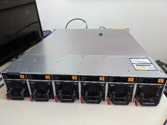 |
| 1 x Intel FPGA Download Cable II (Only Required for manual flashing) |  |
| 1 x 2x5 Extension header - Samtech Part No: ESQ-105-13-L-D (Only Required for manual flashing) | 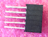 |
The following table highlights the versions of the software which compose the OFS stack. The installation of the OPAE SDK on top of the Linux DFL drivers will be discussed in their relevant sections in this document.
Table 4: Software Version Summary
| Component | Version |
|---|---|
| FPGA Platform | Intel® FPGA SmartNIC N6001-PL, release notes: https://github.com/OFS/ofs-n6001/releases/tag/ofs-2023.2-1 under "Known Issues" |
| OPAE SDK | 2.8.0-1 |
| Kernel Drivers | ofs-2023.2-6.1-1 |
| OneAPI-ASP | ofs-2023.2-1 |
| OFS FIM Source Code for N6001 | ofs-2023.2-1 |
| OFS FIM Common Resources | Tag: ofs-fim-common-1.1.0-rc2 |
| OFS Platform AFU BBB | ofs-2023.2-1 |
| Intel Quartus Prime Pro Edition Design Software* | Quartus Prime Pro Version 23.2 for Linux |
| Operating System | RedHatEnterprise Linux® (RHEL) 8.6 |
The following table highlights the differences between N6000/1 PL FPGA SmartNIC platforms (SKU1/SKU2). Use this table to identify which version of the N6000/1-PL FPGA SmartNIC platform you have. The board identification printed by the fpgainfo fme commands depends on both the OPAE SDK and Linux DFL drivers from sections 3.0 OFS DFL Kernel Drivers through 4.0 OPAE Software Development Kit to be installed before it can be run.
Table 5: Intel N6000/1-PL FPGA SmartNIC Platform SKU Mapping
| SKU Mapping | SKU Value | Primary Difference | fpgainfo Identification |
|---|---|---|---|
| N6000 | Q1613314XXXXX | PCIe Gen 4 1x16 mechanical bifurcated 2x8 logical to host, with one PCIe Gen 4x8 endpoint reserved for Intel E810-C-CAM2 NIC, the other reserved for FIM | "Intel Acceleration Development Platform N6000" |
| N6001 | Q0216514XXXXX | PCIe Gen 4 1x16 mechanical and logical connection between host and FIM | "Intel Acceleration Development Platform N6001" |
The following table highlights the programmable firmware versions that are supported on the Intel N6001-PL FPGA SmartNIC Platform in the OFS 2023.1 release. Programming and verifying these components is discussed in their respective sections.
Table 6: Intel® FPGA SmartNIC N6001-PL Programmable Component Version Summary
| Component | Version |
|---|---|
| PR Interface ID | d8fd88a7-8683-57ba-8be6-a1e058b7d4ed |
| Bitstream ID | 360571655605884772 |
| BMC RTL | 3.14.0 |
| BMC NIOS FW | 3.14.0 |
1.7 Initial Server Setup
1.7.1 Server BMC and BIOS Updates
Both the server BIOS and BMC need to match the versions listed below in Table 7: Supermicro Server BMC BKC. These updates only apply for this specific Best Known Configuration (BKC) - other server manufacturers may require different BIOS updates. Please consult your server's user guide and release notes for update information.
Information about the server’s currently loaded firmware can be found on the BMC web portal dashboard. Accessing this page requires an Ethernet cable to be attached to an open port on the server labelled “IPMI”. During boot the BMC’s login IP will be presented on the screen.
Open this IP address in a browser and enter your login credentials. The default username is ADMIN, and the default password has been printed on the service tag that pulls out from the front of the server case. It is recommended the user change their BMC’s default username as soon as they are able
After logging in you should be able to review information about the BMC and BIOS by referring to the System box, visible upon initial loading of the page. Double check that the values match those in Table 7 Supermicro Server BMC BKC. If they do not, you may download the appropriate versions from the Supermicro product page by selecting the BIOS option and downloading the most recent “Bundled Software File Name”. Follow the BMC and BIOS update instructions included in the Supermicro manuals page in the document X12/H12 BMC Manual in Appendix A.2 Updating Firmware Using BMC Web GUI.
If using a different server model, refer to that server’s user guide for instructions on remote system management.
Table 7: Supermicro Server BMC BKC
| Component | Version |
|---|---|
| BIOS Version | American Megatrends International, LLC(1.4) |
1.7.2 Server Fan Speed
The recommended fan speed setting is to use the 100% preset. If using a different server model, refer to that server’s user guide for instructions on changing fan speed. The following steps will help users on the Supermicro platform.
- Log in to the Supermicro server BMC. (This requires an Ethernet cable to be attached to an open port on the server labelled “IPMI”.)
- During boot the BMC’s login IP will be presented on the screen. Open this IP address in a browser and enter your login credentials. The default username is ADMIN, and the default password has been printed on the service tag that pulls out from the front of the server case.
- On the left menu select System -> Component Info, select the Fan tab, under Advanced Settings click the circle next to Full Speed.
1.7.3 Server BIOS Configuration Changes
To enter the Supermicro server’s BIOS setup page, reboot, and press \<Delete> when prompted. You can browse the tabs / options with a combination of arrow keys along with \<Escape> and \<Enter>.
1.7.3.1 Enabling Intel VT-d Technology
Navigate right to the Advanced tab, then select the following menu options: Chipset Configuration -> North Bridge -> IIO Configuration -> Intel VT for Directed I/O (VT-d). If not already, enable the option Intel VT for Directed I/O (VT-d).
1.7.3.2 PCie Slot Mapping
The Intel N6001-PL FPGA SmartNIC Platform is officially verified in the upper middle PCIe x16 slot (Slot 3). If using a different slot, refer to the information in Table 8 PCIe Slot Mapping for which port to manually change in the server BIOS.
Table 8: PCIe Slot Mapping
| CPU Number | Port Number (in BIOS) | PCIe Slot |
|---|---|---|
| CPU1 | Port 2 | 5 and 6 |
| CPU1 | Port 4 | 7 and 8 |
| CPU2 | Port 2 | 1 and 2 |
| CPU2 | Port 4 | 3 and 4 |
1.7.4 Intel® FPGA SmartNIC N6001-PL Installation Procedure
The following instructions will help to ensure safe installation of the Intel® FPGA SmartNIC N6001-PL into a supported server. Refer to Table 8 PCIe Slot Mapping for a breakdown of the available PCIe slots on a SuperMicro SYS-220HE.
- Position the board over the selected connector on the motherboard.
- Press down gently and firmly to seat the card in the PCIe slot, and then secure the bracket to the system chassis with the retention screw.

Table 9: Intel® FPGA SmartNIC N6001-PL Installation Procedure
| Callout | Description |
|---|---|
| 1 | Retention screw |
| 2 | Press down here gently |
| 3 | Press down here gently |
| 4 | Motherboard |
Do not bend the card while inserting into a slot. Do not apply much pressure in regions 2 or 3 while inserting.
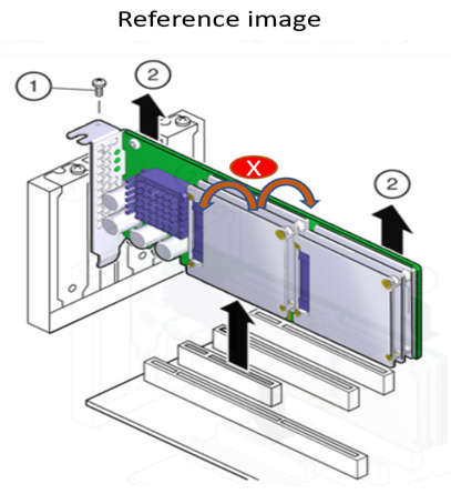
1.7.5 Intel® FPGA SmartNIC N6001-PL Removal Procedure
The following instructions will help to ensure safe removal of the platform from a supported server.
- Disconnect all power cords from the server power supply(s).
- Remove the retention bracket screw.
- Carefully lift the card out of the PCIe slot.
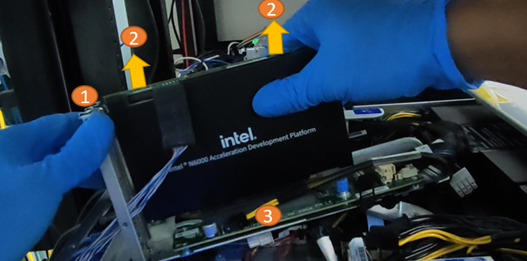
Table 10: Intel® FPGA SmartNIC N6001-PL Removal Procedure
| Callout | Description |
|---|---|
| 1 | Retention screw |
| 2 | Pull up here gently |
| 3 | Motherboard |
Do not bend the card while removing it from the slot.
2.0 OFS Stack Architecture Overview for Reference Platform
2.1 Hardware Components
The OFS hardware architecture decomposes all designs into a standard set of modules, interfaces, and capabilities. Although the OFS infrastructure provides a standard set of functionality and capability, the user is responsible for making the customizations to their specific design in compliance with the specifications outlined in the FPGA Interface Manager Technical Reference Manual: Intel Open FPGA Stack for Intel Agilex FPGA.
OFS is a hardware and software infrastructure that provides an efficient approach to developing a customer FPGA-based platform or workload using an Intel, 3rd party, or custom board.
2.1.1 FPGA Interface Manager
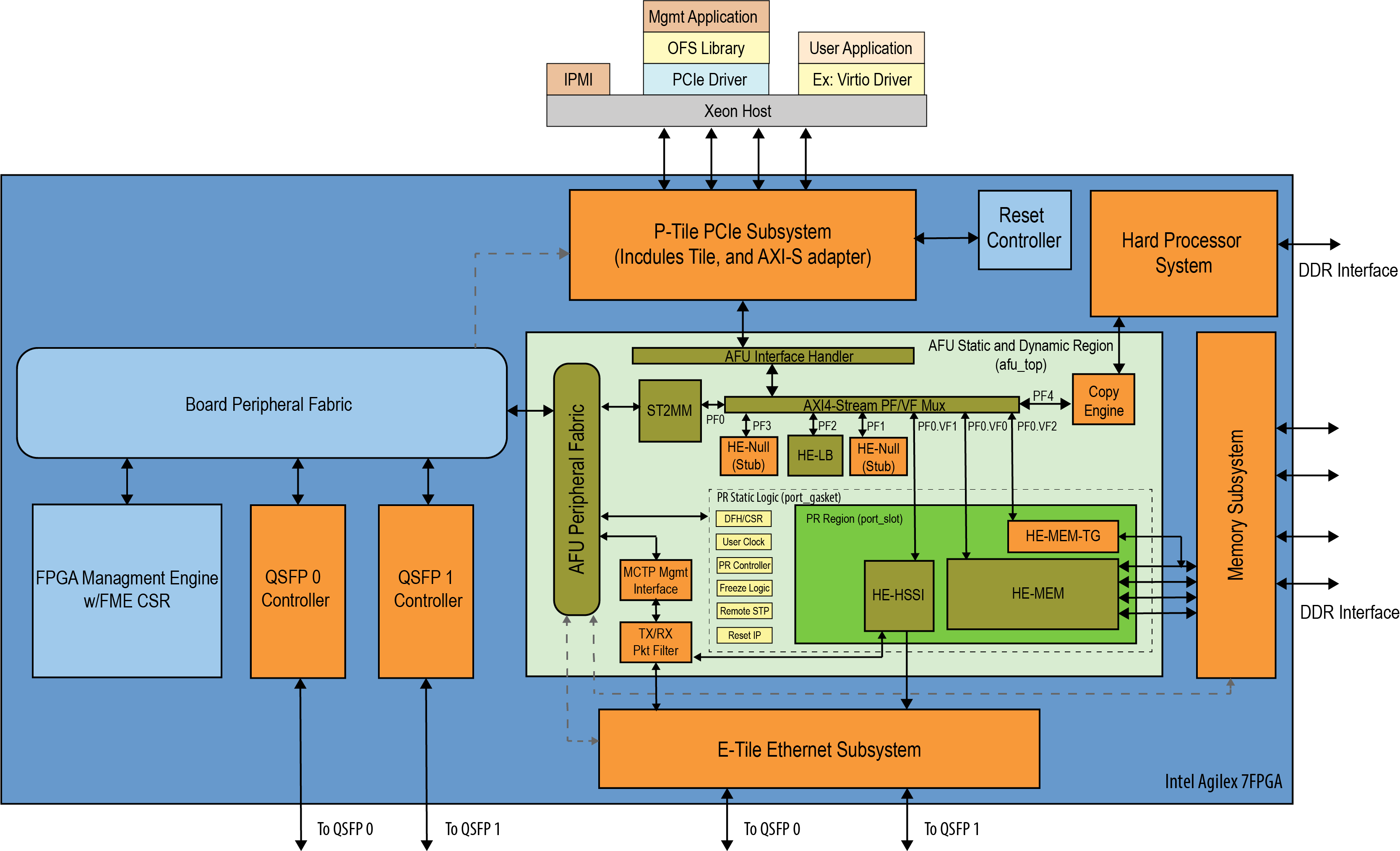
The FPGA Interface Manager (FIM), or shell of the FPGA provides platform management functionality, clocks, resets, and interface access to the host and peripheral features on the acceleration platform. The OFS architecture for Intel Agilex FPGA provides modularity, configurability and scalability. The primary components of the FPGA Interface Manager or shell of the reference design are:
- PCIe Subsystem - a hierarchical design that targets the P-tile PCIe hard IP and is configured to support Gen4 speeds and Arm AXI4-Stream Data Mover functional mode.
- Ethernet Subsystem - provides portability to different Ethernet configurations across platforms and generations and reusability of the hardware framework and software stack.
- Memory Subsystem - composed of 5 DDR4 channels; two HPS DDR4 banks, x40 (x32 Data and x8 ECC), 1200 MHz, 1GB each, and four Fabric DDR4 banks, x32 (no ECC), 1200 MHz, 4GB
- Hard Processor System - 64-bit quad core ARM® Cortex*-A53 MPCore with integrated peripherals.
- Reset Controller
- FPGA Management Engine - Provides a way to manage the platform and enable acceleration functions on the platform.
- AFU Peripheral Fabric for AFU accesses to other interface peripherals
- Board Peripheral Fabric for master to slave CSR accesses from Host or AFU
- Platform Management Controller Interface (PMCI) to the board management controller
The FPGA Management Engine (FME) provides management features for the platform and the loading/unloading of accelerators through partial reconfiguration. Each feature of the FME exposes itself to the kernel-level OFS drivers on the host through a Device Feature Header (DFH) register that is placed at the beginning of Control Status Register (CSR) space. Only one PCIe link can access the FME register space in a multi-host channel design architecture at a time.
Note: For more information on the FIM and its external connections, refer to the FPGA Interface Manager Technical Reference Manual: Intel Open FPGA Stack for Intel Agilex FPGA.
2.1.2 AFU
An AFU is an acceleration workload that interfaces to the FIM. The AFU boundary in this reference design comprises both static and partial reconfiguration (PR) regions. You can decide how you want to partition these two areas or if you want your AFU region to only be a partial reconfiguration region. A port gasket within the design provides all the PR specific modules and logic required to support partial reconfiguration. Only one partial reconfiguration region is supported in this design.
Similar to the FME, the port gasket exposes its capability to the host software driver through a DFH register placed at the beginning of the port gasket CSR space. In addition, only one PCIe link can access the port register space.
You can compile your design in one of the following ways:
- Your entire AFU resides in a partial reconfiguration region of the FPGA.
- The AFU is part of the static region and is compiled as a flat design.
- Your AFU contains both static and PR regions.
In this design, the AFU region is comprised of:
- AFU Interface handler to verify transactions coming from AFU region.
- PF/VF Mux to route transactions to and from corresponding AFU components: ST2MM module, Virtio LB stub, PCIe loopback host exerciser (HE-LB), HSSI host exerciser (HE-HSSI), Memory Host Exerciser (HE-MEM), Traffic Generator to memory (HE-MEM-TG), Port Gasket (PRG) and HPS Copy Engine.
- AXI4 Streaming to Memory Map (ST2MM) Module that routes MMIO CSR accesses to FME and board peripherals.
- Host exercisers to test PCIe, memory and HSSI interfaces (these can be removed from the AFU region after your FIM design is complete to provide more resource area for workloads)
- Basic HPS Copy Engine to copy second-stage bootloader and Linux OS image from Host DDR to HPS DDR.
- Port gasket and partial reconfiguration support.
- Component for handling PLDM over MCTP over PCIe Vendor Defined Messages (VDM)
The AFU has the option to consume native packets from the host or interface channels or to instantiate a shim provided by the Platform Interface Manager (PIM) to translate between protocols.
Note: For more information on the Platform Interface Manager and AFU development and testing, refer to the AFU Development Guide: OFS for Intel® Agilex® PCIe Attach FPGAs.
2.2 OFS Software Overview
The responsibility of the OFS kernel drivers is to act as the lowest software layer in the FPGA software stack, providing a minimalist driver implementation between the host software and functionality that has been implemented on the development platform. This leaves the implementation of IP-specific software in user-land, not the kernel. The OFS software stack also provides a mechanism for interface and feature discovery of FPGA platforms.
The OPAE SDK is a software framework for managing and accessing programmable accelerators (FPGAs). It consists of a collection of libraries and tools to facilitate the development of software applications and accelerators. The OPAE SDK resides exclusively in user-space, and can be found on the OPAE SDK Github.
The OFS drivers decompose implemented functionality, including external FIM features such as HSSI, EMIF and SPI, into sets of individual Device Features. Each Device Feature has its associated Device Feature Header (DFH), which enables a uniform discovery mechanism by software. A set of Device Features are exposed through the host interface in a Device Feature List (DFL). The OFS drivers discover and "walk" the Device Features in a Device Feature List and associate each Device Feature with its matching kernel driver.
In this way the OFS software provides a clean and extensible framework for the creation and integration of additional functionalities and their features.
*Note: A deeper dive on available SW APIs and programming model is available in the Software Reference Manual: Intel® Open FPGA Stack and on kernel.org.
3.0 OFS DFL Kernel Drivers
OFS DFL driver software provides the bottom-most API to FPGA platforms. Libraries such as OPAE and frameworks like DPDK are consumers of the APIs provided by OFS. Applications may be built on top of these frameworks and libraries. The OFS software does not cover any out-of-band management interfaces. OFS driver software is designed to be extendable, flexible, and provide for bare-metal and virtualized functionality. An in depth look at the various aspects of the driver architecture such as the API, an explanation of the DFL framework, and instructions on how to port DFL driver patches to other kernel distributions can be found on https://github.com/OPAE/linux-dfl/wiki.
An in-depth review of the Linux device driver architecture can be found on opae.github.io.
3.1 OFS DFL Kernel Driver Environment Setup
All OFS DFL kernel driver code resides in the Linux DFL GitHub repository. This repository is open source and should not require any permissions to access. It includes a snapshot of the Linux kernel with the OFS driver included in /drivers/fpga/*. Downloading, configuration, and compilation will be discussed in this section. The only operating systems supported out of the box by the Linux DFL kernel drivers is RHEL 8.6.
This installation process assumes the user has access to an internet connection in order to clone specific GitHub repositories, and to satisfy package dependencies.
1. Make the following changes on your installation machine to satisfy all dependencies:
If you wish to install the pre-built linux-dfl package available on the OFS 2023.1 Release Page skip to section 3.3 Installing the OFS DFL Kernel Drivers from Pre-Built Packages.
2. You must satisfy the following package dependencies if building and installing the drivers from source. Double check that all packages have been found and installed. The following section assumes you require use of a proxy to download from remote repositories. If you do not, then you may safely ignore all references to proxies in the following code block.
# If you require the use of a proxy, add it to DNF using by editing the following file
$ sudo nano /etc/dnf/dnf.conf
# Include your proxy by adding the following line, replacing the URL with your proxy's URL
# proxy=http://proxy.server.com:port
$ sudo dnf update
$ subscription-manager repos --enable codeready-builder-for-rhel-8-x86_64-rpms
$ sudo dnf install https://dl.fedoraproject.org/pub/epel/epel-release-latest-8.noarch.rpm
$ sudo dnf install -y python3 python3-pip python3-devel \
gdb vim git gcc gcc-c++ make cmake libuuid-devel rpm-build systemd-devel nmap \
python3-jsonschema json-c-devel tbb-devel rpmdevtools libcap-devel \
python3-pyyaml hwloc-devel libedit-devel git kernel-headers kernel-devel elfutils-libelf-devel ncurses-devel openssl-devel bison flex cli11-devel spdlog-devel
$ python3 -m pip install --user jsonschema virtualenv pudb pyyaml
$ sudo pip3 uninstall setuptools
$ sudo pip3 install Pybind11==2.10.0 --proxy http://yourproxy:xxx
$ sudo pip3 install setuptools==59.6.0 --prefix=/usr --proxy http://yourproxy:xxx
$ wget http://ftp.pbone.net/mirror/archive.fedoraproject.org/epel/8.4/Everything/x86_64/Packages/p/pybind11-devel-2.4.3-2.el8.x86_64.rpm
$ wget http://ftp.pbone.net/mirror/archive.fedoraproject.org/epel/8.4/Everything/x86_64/Packages/p/python3-pybind11-2.4.3-2.el8.x86_64.rpm
$ sudo dnf localinstall ./python3-pybind11-2.4.3-2.el8.x86_64.rpm ./pybind11-devel-2.4.3-2.el8.x86_64.rpm -y
It is recommended you create an empty top level directory for your OFS related repositories to keep the working environment clean. All steps in this installation will use a generic top-level directory at /home/OFS/. If you have created a different top-level directory, replace this path with your custom path.
3. Initialize an empty git repository and clone the LTS tagged DFL driver source code:
$ mkdir /home/OFS/
$ cd /home/OFS/
$ git init
$ git clone https://github.com/OFS/linux-dfl
$ cd /home/OFS/linux-dfl
$ git checkout tags/ofs-2023.2-6.1-1
4. Verify that the correct tag/branch have been checkout out.
Note: If two different tagged releases are tied to the same commit, running git describe tags may report the other release's tag. This is why the match is made explicit.
Note: The linux-dfl repository is roughly 5 GB in size.
3.2 Building and Installing the OFS DFL Kernel Drivers from Source
1. The following set of instructions walk you through copying an existing kernel configuration file on your machine and changing the minimal required configuration settings.:
$ cd /home/OFS/linux-dfl
$ cp /boot/config-`uname -r` .config
$ cat configs/dfl-config >> .config
$ echo 'CONFIG_LOCALVERSION="-dfl"' >> .config
$ echo 'CONFIG_LOCALVERSION_AUTO=y' >> .config
$ sed -i -r 's/CONFIG_SYSTEM_TRUSTED_KEYS=.*/CONFIG_SYSTEM_TRUSTED_KEYS=""/' .config
$ sed -i '/^CONFIG_DEBUG_INFO_BTF/ s/./#&/' .config
$ echo 'CONFIG_DEBUG_ATOMIC_SLEEP=y' >> .config
$ export LOCALVERSION=
$ make olddefconfig
1.1. The above command may report errors resembling symbol value 'm' invalid for CHELSIO_IPSEC_INLINE. These errors indicate that the nature of the config has changed between the currently executing kernel and the kernel being built. The option "m" for a particular kernel module is no longer a valid option, and the default behavior is to simply turn the option off. However the option can likely be turned back on by setting it to 'y'. If the user wants to turn the option back on, change it to 'y' and re-run "make olddefconfig":
(Optional) To use the built-in GUI menu for editing kernel configuration parameters, you can opt to run make menuconfig.
2. Linux kernel builds take advantage of multiple processors to parallelize the build process. Display how many processors are available with the nproc command, and then specify how many make threads to utilize with the -j option. Note that number of threads can exceed the number of processors. In this case, the number of threads are set to the number of processors in the system.
3. The following options are available to build a set of packages. The package options for this flow as as follows:
- rpm-pkg: Build both source and binary RPM kernel packages
- binrpm-pkg: Build only the binary kernel RPM package
- deb-pkg: Build both source and binary deb kernel packages
- bindeb-pkg: Build only the binary kernel deb package
If you are concerned about the size of the resulting package and binaries, they can significantly reduce the size of the package and object files by using the make variable INSTALL_MOD_STRIP. If this is not a concern, feel free to skip this step. The below instructions will build a set of binary RPM packages:
4. By default a directory is created in your home directory called rpmbuild. This directory will house all of the kernel packages which have been built. You need to navigate to the newly built kernel packages and install them. The following files were generated using the build command executed in the previous step:
$ cd ~/rpmbuild/RPMS/x86_64
$ ls
kernel-6.1.41_dfl.x86_64.rpm kernel-headers-6.1.41_dfl.x86_64.rpm
$ sudo dnf localinstall kernel*.rpm
5. The system will need to be rebooted in order for changes to take affect. After a reboot, select the newly built kernel as the boot target. This can be done pre-boot using the command grub2-reboot, which removes the requirement for user intervention. After boot, verify that the currently running kernel matches expectation.
6. Verify the DFL drivers have been successfully installed by reading version information directly from /lib/modules. Recall that the name of the kernel built as apart of this section is 6.1.41-dfl. If the user set a different name for their kernel, change this path as needed:
$ cd /usr/lib/modules/6.1.41-dfl/kernel/drivers/fpga
$ ls
dfl-afu.ko dfl-fme.ko dfl-fme-region.ko dfl.ko dfl-pci.ko fpga-mgr.ko intel-m10-bmc-sec-update.ko
dfl-fme-br.ko dfl-fme-mgr.ko dfl-hssi.ko dfl-n3000-nios.ko fpga-bridge.ko fpga-region.ko
If an N6000/1-PL FPGA SmartNIC Platform is present on the server, you can also double check driver versions using the lsmod command:
$ lsmod | grep dfl
uio_dfl 20480 0
dfl_emif 16384 0
uio 20480 1 uio_dfl
ptp_dfl_tod 16384 0
dfl_intel_s10_iopll 20480 0
8250_dfl 20480 0
dfl_fme_region 20480 0
dfl_fme_br 16384 0
dfl_fme_mgr 20480 2
dfl_fme 49152 0
dfl_afu 36864 0
dfl_pci 20480 0
dfl 40960 11 dfl_pci,uio_dfl,dfl_fme,intel_m10_bmc_pmci,dfl_fme_br,8250_dfl,qsfp_mem,ptp_dfl_tod,dfl_afu,dfl_intel_s10_iopll,dfl_emif
fpga_region 20480 3 dfl_fme_region,dfl_fme,dfl
fpga_bridge 20480 4 dfl_fme_region,fpga_region,dfl_fme,dfl_fme_br
fpga_mgr 20480 4 dfl_fme_region,fpga_region,dfl_fme_mgr,dfl_fme
Refer to the following table for a brief description of each driver:
Table 11: DFL Driver Modules
| Module Name | Short Description |
|---|---|
| uio_dfl | Generic DFL driver for Userspace I/O devices |
| dfl_intel_s10_iopll | DFL Intel S10 IOPLL driver |
| uio | UIO Driver |
| dfl_fme_region | FPGA Region for DFL FPGA Management Engine |
| ptp_dfl_tod | DFL ToD driver |
| dfl_emif | DFL EMIF driver |
| dfl_fme_br | FPGA Bridge for DFL FPGA Management Engine |
| 8250_dfl | DFL Intel UART driver |
| dfl_fme_mgr | FPGA Manager for DFL FPGA Management Engine |
| dfl_fme | FPGA Management Engine driver |
| dfl_afu | FPGA Accelerated Function Unit driver |
| dfl_pci | FPGA DFL PCIe Device Driver |
| dfl | FPGA Device Feature List (DFL) Support |
| fpga_region | FPGA Region Driver |
| fpga_bridge | FPGA Bridge Driver |
| fpga_mgr | FPGA manager framework |
7. Two kernel parameters must be added to the boot commandline for the newly installed kernel. First, open the file grub:
8. In the variable GRUB_CMDLINE_LINUX add the following parameters in bold: GRUB_CMDLINE_LINUX="crashkernel=auto resume=/dev/mapper/cl-swap rd.lvm.lv=cl/root rd.lvm.lv=cl/swap rhgb quiet intel_iommu=on pcie=realloc hugepagesz=2M hugepages=200"
Note: If you wish to instead set hugepages on a per session bassis, you can perform the following steps. These settings will be lost on reboot.
$ mkdir -p /mnt/huge
$ mount -t hugetlbfs nodev /mnt/huge
$ echo 2048 > /sys/devices/system/node/node0/hugepages/hugepages-2048kB/nr_hugepages
$ echo 2048 > /sys/devices/system/node/node1/hugepages/hugepages-2048kB/nr_hugepages
9. Save your edits, then apply them to the GRUB2 configuration file.
10. Warm reboot. Your kernel parameter changes should have taken affect.
$ cat /proc/cmdline
BOOT_IMAGE=(hd1,gpt2)/vmlinuz-6.1.41-dfl root=/dev/mapper/cl-root ro crashkernel=auto resume=/dev/mapper/cl-swap rd.lvm.lv=cl/root rd.lvm.lv=cl/swap intel_iommu=on pcie=realloc hugepagesz=2M hugepages=200 rhgb quiet
3.3 Installing the OFS DFL Kernel Drivers from Pre-Built Packages
1. Make the following changes on your installation machine to satisfy all dependencies:
2. To use the pre-built Linux DFL packages, the user will need to download the files from the OFS 2023.1 Release Page. You can choose to either install using the SRC RPMs, or to use the pre-built RPM packages targeting the official supported release platform.
$ tar xf kernel-6.1.41_dfl-1.x86_64-<<version>>.tar.gz
$ sudo dnf localinstall kernel-6.1.41_dfl_<<version>>.x86_64.rpm \
kernel-devel-6.1.41_dfl_<<version>>.x86_64.rpm \
kernel-headers-6.1.41_dfl_<<version>>.x86_64.rpm
### OR
$ sudo dnf localinstall kernel-6.1.41_dfl_<<version>>.src.rpm
3. After installation has completed you should continue with steps 4-9 in previous section 3.2 Building and Installing the OFS DFL Kernel Drivers from Source.
4.0 OPAE Software Development Kit
The OPAE SDK software stack sits in user space on top of the OFS kernel drivers. It is a common software infrastructure layer that simplifies and streamlines integration of programmable accelerators such as FPGAs into software applications and environments. OPAE consists of a set of drivers, user-space libraries, and tools to discover, enumerate, share, query, access, manipulate, and reconfigure programmable accelerators. OPAE is designed to support a layered, common programming model across different platforms and devices. To learn more about OPAE, its documentation, code samples, an explanation of the available tools, and an overview of the software architecture, visit the opae reference page.
The OPAE SDK source code is contained within a single GitHub repository hosted at the OPAE Github. This repository is open source and does not require any permissions to access. You have two options to install OPAE as discussed below - using pre-built packages offered by Intel, or building the source code locally.
4.1 OPAE SDK Build Environment Setup
This installation process assumes the you have access to an internet connection in order to pull specific GitHub repositories, and to satisfy package dependencies.
1. Before OPAE SDK installation you must remove any prior OPAE frameworks. To remove these packages:
2. The following repository changes must be enabled in order to install all dependencies:
$ subscription-manager release --set=8.6
$ sudo dnf update
$ subscription-manager repos --enable codeready-builder-for-rhel-8-x86_64-rpms
$ sudo dnf install https://dl.fedoraproject.org/pub/epel/epel-release-latest-8.noarch.rpm
It is recommended you create an empty top level directory for their OFS related repositories to keep the working environment clean. All steps in this installation will use a generic top-level directory at /home/OFS/. If the you have created a different top-level directory, replace this path with your custom path.
3. Initialize an empty git repository and clone the tagged OPAE SDK source code:
$ cd /home/OFS/
$ git init
$ git clone https://github.com/OFS/opae-sdk opae-sdk
$ cd /home/OFS/opae-sdk
$ git checkout tags/2.8.0-1
5. Verify that the correct tag/branch have been checkout out.
4.2 Installing the OPAE SDK with Pre-Built Packages
You can skip the entire build process and use a set of pre-built binaries supplied by Intel. Visit the OFS ofs-2023.2-1 Release Page and navigate to the bottom of the page, under the Assets tab you will see a file named opae-2.8.0-1.x86_64-<
$ dnf install --enablerepo=codeready-builder-for-rhel-8-x86_64-rpms -y python3 python3-pip python3-devel python3-jsonschema python3-pyyaml git gcc gcc-c++ make cmake libuuid-devel json-c-devel hwloc-devel tbb-devel cli11-devel spdlog-devel libedit-devel systemd-devel doxygen python3-sphinx pandoc rpm-build rpmdevtools python3-virtualenv yaml-cpp-devel libudev-devel libcap-devel

$ pip3 install --upgrade --prefix=/usr pip setuptools pybind11

$ tar xf opae-2.8.0-1.x86_64-<<date>>_<<build>>.tar.gz
For a fast installation you can delete the source RPM as it isn't necessary, and install all remaining OPAE RPMs:
4.3 Building and Installing the OPAE SDK by Script
1. Build the OPAE SDK source code, and pack it into several local RPM packages. Building the code into packages allows for easier installation and removal. This build script can take advantage of multiple processors to parallelize the build process. Display how many processors are available with the $(nproc) command, and then specify how many make threads to utilize with the -j option. Note that number of threads can exceed the number of processors. In this case, the number of threads are set to the number of processors in the system.
cd /home/OFS/

$ podman pull registry.access.redhat.com/ubi8:8.6
$ podman run -ti -v "$PWD":/src:Z -w /src registry.access.redhat.com/ubi8:8.6

# Everything after runs within container:

# Enable EPEL
$ dnf install -y https://dl.fedoraproject.org/pub/epel/epel-release-latest-8.noarch.rpm

$ dnf install --enablerepo=codeready-builder-for-rhel-8-x86_64-rpms -y python3 python3-pip python3-devel python3-jsonschema python3-pyyaml git gcc gcc-c++ make cmake libuuid-devel json-c-devel hwloc-devel tbb-$ devel cli11-devel spdlog-devel libedit-devel systemd-devel doxygen python3-sphinx pandoc rpm-build rpmdevtools python3-virtualenv yaml-cpp-devel libudev-devel libcap-devel

$ pip3 install --upgrade --prefix=/usr pip setuptools pybind11

$ ./opae-sdk/packaging/opae/rpm/create unrestricted

$ exit
2. After a successful compile there should be packages generated:
The below table lists a short description for each package:
Table 12: OPAE Package Description
| Package Name | Description |
|---|---|
| opae | OPAE SDK is a collection of libraries and tools to facilitate the development of software applications and accelerators using OPAE. It provides a library implementing the OPAE C API for presenting a streamlined and easy-to-use interface for software applications to discover, access, and manage FPGA devices and accelerators using the OPAE software stack. |
| opae-debuginfo | This package provides debug information for package opae. Debug information is useful when developing applications that use this package or when debugging this package. |
| opae-debugsource | This package provides debug sources for package opae. Debug sources are useful when developing applications that use this package or when debugging this package. |
| opae-devel | OPAE headers, tools, sample source, and documentation |
| opae-devel-debuginfo | This package provides debug information for package opae-devel. Debug information is useful when developing applications that use this package or when debugging this package. |
| opae-tools | This package contains OPAE base tools binaries |
| opae-extra-tools | Additional OPAE tools |
| opae-extra-tools-debuginfo | This package provides debug information for package opae-extra-tools. Debug information is useful when developing applications that use this package or when debugging this package. |
3. Install the OPAE SDK packages:
$ cd /home/OFS/opae-sdk/packaging/opae/rpm
$ rm -rf opae-2.8.0-1.el8.src.rpm
$ sudo dnf localinstall -y opae*.rpm
4. Check that all packages have been installed:
$ rpm -qa | grep opae
opae-packager-2.8.0-1.x86_64
opae-devel-2.8.0-1.x86_64
opae-PACSign-2.8.0-1.x86_64
opae-tools-extra-2.8.0-1.x86_64
opae-2.8.0-1.x86_64
opae-tools-2.8.0-1.x86_64
opae-libs-2.8.0-1.x86_64
opae-opae.admin-2.8.0-1.x86_64
opae-tests-2.8.0-1.x86_64
4.4 OPAE Tools Overview
The following section offers a brief introduction including expected output values for the utilities included with OPAE. A full explanation of each command with a description of its syntax is available in the opae-sdk GitHub repo.
4.4.1 Board Management with fpgainfo
The fpgainfo utility displays FPGA information derived from sysfs files.
Displays FPGA information derived from sysfs files. The command argument is one of the following: errors, power, temp, port, fme, bmc, phy or mac, security. Some commands may also have other arguments or options that control their behavior.
For systems with multiple FPGA devices, you can specify the BDF to limit the output to the FPGA resource with the corresponding PCIe configuration. If not specified, information displays for all resources for the given command.
Note: Your BItstream ID and PR Interface Id may not match the below examples.
The following examples walk through sample outputs generated by fpgainfo.
$ sudo fpgainfo fme

Intel Acceleration Development Platform N6001
Board Management Controller NIOS FW version: 3.14.0
Board Management Controller Build version: 3.14.0
//****** FME ******//
Object Id                        : 0xED00001
PCIe s:b:d.f                     : 0000:B1:00.0
Vendor Id                        : 0x8086
Device Id                        : 0xBCCE
SubVendor Id                     : 0x8086
SubDevice Id                     : 0x1771
Socket Id                        : 0x00
Ports Num                        : 01
Bitstream Id                     : 360571655605884772
Bitstream Version                : 5.0.1
Pr Interface Id                  : d8fd88a7-8683-57ba-8be6-a1e058b7d4ed
Boot Page                        : user1
Factory Image Info               : a2b5fd0e7afca4ee6d7048f926e75ac2
User1 Image Info                 : d8fd88a7-8683-57ba-8be6-a1e058b7d4ed
User2 Image Info                 : d8fd88a7-8683-57ba-8be6-a1e058b7d4ed
$ sudo fpgainfo bmc

Intel Acceleration Development Platform N6001
Board Management Controller NIOS FW version: 3.14.0
Board Management Controller Build version: 3.14.0
//****** FME ******//
Object Id                        : 0xED00001
PCIe s:b:d.f                     : 0000:B1:00.0
Vendor Id                        : 0x8086
Device Id                        : 0xBCCE
SubVendor Id                     : 0x8086
SubDevice Id                     : 0x1771
Socket Id                        : 0x00
Ports Num                        : 01
Bitstream Id                     : 360571655605884772
Bitstream Version                : 5.0.1
Pr Interface Id                  : d8fd88a7-8683-57ba-8be6-a1e058b7d4ed
( 1) VCCRT_GXER_0V9 Voltage                             : 0.91 Volts
( 2) FPGA VCCIO_1V2 Voltage                             : 1.21 Volts
( 3) Inlet 12V Aux Rail Current                         : 0.87 Amps
( 4) FPGA E-Tile Temperature [Remote]                   : 47.00 Celsius
( 5) AVDD_ETH_0V9_CVL Voltage                           : 1.48 Volts
( 6) FPGA E-TILE Temperature #3                         : 51.00 Celsius
...
(77) FPGA FABRIC Remote Digital Temperature#3           : 47.00 Celsius
(78) MAX10 & Board CLK PWR 3V3 Inlet Current            : 0.97 Amps
(79) CVL Non Core Rails Inlet Current                   : 0.01 Amps
(80) FPGA Core Voltage Phase 0 VR Temperature           : 49.50 Celsius
4.4.2 Sensor Monitoring with fpgad
The fpgad is a service that can help you protect the server from crashing when the hardware reaches an upper non-recoverable or lower non-recoverable sensor threshold (also called as fatal threshold). The fpgad is capable of monitoring each of the 80 sensors reported by the Board Management Controller. This service is only available once the installation instructions in sections 3.2 Building and Installing the OFS DFL Kernel Drivers and 4.1 OPAE SDK Build Environment Setup have been completed . Note: Qualified OEM server systems should provide the required cooling for your workloads. Therefore, using fpgad may be optional.
When the opae-tools-extra-2.8.0-1.x86_64 package is installed, fpgad is placed in the OPAE binaries directory (default: /usr/bin). The configuration file fpgad.cfg is located at /etc/opae. The log file fpgad.log which monitors fpgad actions is located at /var/lib/opae/. The fpgad periodically reads the sensor values and if the values exceed the warning threshold stated in the fpgad.conf or the hardware defined warning threshold, it masks the PCIe Advanced Error Reporting (AER) registers for the Intel N6000/1-PL FPGA SmartNIC Platform to avoid system reset. Use the following command to start the fpgad service:
Use the following command to start the fpgad service:
The configuration file only includes the threshold setting for critical sensor 12V Aux Rail Voltage (sensor 29). This sensor does not have a hardware defined warning threshold and hence fpgad relies on the configuration file. The fpgad uses information contained within this file to mask the PCIe AER register when the sensor reaches the warning threshold.You may create another entry below the 12V Aux Voltage entry for any other sensors on the board. The updated configuration file includes a new entry for (18) Board Front Side Temperature with arbitrary values:
{
"configurations": {
    "fpgad-xfpga": {
        "configuration": {
        },
        "enabled": true,
        "plugin": "libfpgad-xfpga.so",
        "devices": [
            [ "0x8086", "0xbcc0" ],
            [ "0x8086", "0xbcc1" ]
        ]
    },
    "fpgad-vc": {
        "configuration": {
            "cool-down": 30,
            "get-aer": [
                "setpci -s %s ECAP_AER+0x08.L",
                "setpci -s %s ECAP_AER+0x14.L"
            ],
            "disable-aer": [
                "setpci -s %s ECAP_AER+0x08.L=0xffffffff",
                "setpci -s %s ECAP_AER+0x14.L=0xffffffff"
            ],
            "set-aer": [
                "setpci -s %s ECAP_AER+0x08.L=0x%08x",
                "setpci -s %s ECAP_AER+0x14.L=0x%08x"
            ],
            "config-sensors-enabled": true,
            "sensors": [
                {
                    "name": "12V AUX Voltage",
                    "low-warn": 11.40,
                    "low-fatal": 10.56
                },
                {
                    “name”: “3V3 VR Temperature”,
                    “low-warn”: 50.00,
                    “low-fatal”: 100.00

                }
            ]
        },
        "enabled": true,
        "plugin": "libfpgad-vc.so",
        "devices": [
            [ "0x8086", "0x0b30" ],
            [ "0x8086", "0x0b31" ],
            [ "0x8086", "0xaf00" ],
            [ "0x8086", "0xbcce" ]
            ]
    }
},
"plugins": [
    "fpgad-xfpga",
    "fpgad-vc"
]
}
You can monitor the log file to see if upper or lower warning threshold levels are hit. For example:
$ tail -f /var/lib/opae/fpgad.log | grep “sensor.*warning”
fpgad-vc: sensor ' Columbiaville Die Temperature ' warning
You must take appropriate action to recover from this warning before the sensor value reaches upper or lower fatal limits. On reaching the warning threshold limit, the daemon masks the AER registers and the log file will indicate that the sensor is tripped. Sample output: Warning message when the 'CVL Core0 Voltage VR Temperature' exceeds the upper warning threshold limit
$ tail -f /var/lib/opae/fpgad.log
fpgad-vc: sensor 'CVL Core Voltage VR Temperature' warning.
fpgad-vc: saving previous ECAP_AER+0x08 value 0x057ff030 for 0000:b0:02.0
fpgad-vc: saving previous ECAP_AER+0x14 value 0x0000f1c1 for 0000:b0:02.0
fpgad-vc: sensor 'CVL Core Voltage VR Temperature' still tripped.
If the upper or lower fatal threshold limit is reached, then a power cycle of server is required to recover the Intel N6001-PL SmartNIC FPGA Platform. AER is unmasked by the fpgad after the sensor values are within the normal range which is above the lower warning or below the upper warning threshold.
To stop fpgad:
To check status of fpgad:
Optional: To enable fpgad to re-start on boot, execute
For a full list of systemctl commands, run the following command:
4.4.3 Updating with fpgasupdate
The fpgasupdate tool updates the Intel Max10 Board Management Controller (BMC) image and firmware (FW), root entry hash, and FPGA Static Region (SR) and user image (PR). The fpgasupdate tool only accepts images that have been formatted using PACsign. If a root entry hash has been programmed onto the board, then you must also sign the image using the correct keys. Refer to the Security User Guide: Intel Open FPGA Stack for information on created signed images and on programming and managing the root entry hash.
The Intel® FPGA SmartNIC N6001-PL ships with a factory, user1, and user2 programmed image for both the FIM and BMC FW and RTL on all cards. The platform ships with a single FIM image that can be programmed into either user1 or user2, depending in the image selected.
Use the following chart for information on the Bitstream ID and Pr Interface ID, two unique values reported by fpgainfo which can be used to identify the loaded FIM.
Table 13: FIM Version Summary for OFS 2023.1 Release
| FIM Version | Bitstream ID | Pr Interface ID | File Name | Download Location |
|---|---|---|---|---|
| ofs-2023.1 | 360571655605884772 | d8fd88a7-8683-57ba-8be6-a1e058b7d4ed | ofs_top_page[½]_unsigned_user[½].bin | ofs-2023.1 Release Page |
| ofs-n6001-0.9.0-rc2 | 0x50102025AD3DD11 | 92ec8960-2f2f-5544-9804-075d2e8a71a1 | ofs_top_page[½]_unsigned_user[½].bin | ofs-2.3.0 Release Page |
| OFS-2.3.0 | 0x50102022267A9ED | f59830f7-e716-5369-a8b0-e7ea897cbf82 | ofs_top_page[½]_unsigned_user[½].bin | ofs-2.3.0 Release Page |
| OFS-2.2.0 | 0x501020295B081F0 | 8c157a52-1cf2-5d37-9514-944af0a060da | ofs_top_page[½]_unsigned_user[½].bin | ofs-2.2.0-beta Release Page |
Table 14: BMC Version Summary for OFS 2023.1 Release
| BMC FW and RTL Version | File Name | Download Location |
|---|---|---|
| 3.14.0 | AC_BMC_RSU_user_retail_3.14.0_unsigned.rsu | n/a |
-
Example loading a new version of the BMC RTL and FW.
$ sudo fpgasupdate AC_BMC_RSU_user_retail_3.11.0_unsigned.rsu <PCI ADDRESS> [2022-04-14 16:32:47.93] [WARNING ] Update starting. Please do not interrupt. [2022-04-14 16:32:47.93] [INFO ] updating from file /home/user/AC_BMC_RSU_user_retail_3.11.0_unsigned.rsu with size 904064 [2022-04-14 16:32:47.94] [INFO ] waiting for idle [2022-04-14 16:32:47.94] [INFO ] preparing image file [2022-04-14 16:33:26.98] [INFO ] writing image file (100%) [████████████████████] [904064/904064 bytes][Elapsed Time: 0:00:00.00] [2022-04-14 16:33:26.98] [INFO ] programming image file (100%) [████████████████████] [Elapsed Time: 0:00:26.02] [2022-04-14 16:33:53.01] [INFO ] update of 0000:b1:00.0 complete [2022-04-14 16:33:53.01] [INFO ] Secure update OK [2022-04-14 16:33:53.01] [INFO ] Total time: 0:01:05.07 sudo rsu bmcimg -
Example for loading a Static Region (SR) update image. This process will take up to 20 minutes.
$ sudo fpgasupdate ofs_top_page1_unsigned_user1.bin <PCI ADDRESS>
[2022-04-14 16:42:31.58] [WARNING ] Update starting. Please do not interrupt.
[2022-04-14 16:42:31.58] [INFO    ] updating from file ofs_top_page1_pacsign_user1.bin with size 19928064
[2022-04-14 16:42:31.60] [INFO    ] waiting for idle
[2022-04-14 16:42:31.60] [INFO    ] preparing image file
[2022-04-14 16:42:38.61] [INFO    ] writing image file
(100%) [████████████████████] [19928064/19928064 bytes][Elapsed Time: 0:00:16.01]
[2022-04-14 16:42:54.63] [INFO    ] programming image file
(100%) [████████████████████][Elapsed Time: 0:06:16.40]
[2022-04-14 16:49:11.03] [INFO    ] update of 0000:b1:00.0 complete
[2022-04-14 16:49:11.03] [INFO    ] Secure update OK
[2022-04-14 16:49:11.03] [INFO    ] Total time: 0:06:39.45
4.4.4 Signing Images with PACSign
PACSign is an OPAE utility which allows users to insert authentication markers into bitstreams targeted for the Intel® FPGA SmartNIC N6001-PL. PACSign also allows users updating their Static Region (SR) to designate which partition of flash (user1, user2, factory) to overwrite given a specific FIM binary image. All binary images must be signed using PACSign before fpgasupdate can use them for an update. Assuming no Root Entry Hash (REH) has been programmed on the device, the following examples demonstrate how to prepend the required secury authentication data, and specifiy which region of flash to update. More information, including charts detailing the different certification types and their required options, are fully described in the PACsign README on GitHub.
For more information on PACSign and on general security practices surrounding the Intel N6001-PL FPGA SmartNIC device, visit the Security User Guide: Intel Open FPGA Stack.
PACSign can be run on images that have previously been signed. It will overwrite any existing authentication data.
The following example creates an unsigned SR image from an existing signed SR binary update image, targeting the user1 partition in flash.
$ PACSign SR -t UPDATE -s 0 -H openssl_manager -i ofs_top_page1_pacsign_user1.bin -o new_image.bin
No root key specified.  Generate unsigned bitstream? Y = yes, N = no: y
No CSK specified.  Generate unsigned bitstream? Y = yes, N = no: y
No root entry hash bitstream specified.  Verification will not be done.  Continue? Y = yes, N = no: y
2021-10-18 14:42:54,490 - PACSign.log - WARNING - Bitstream is already signed - removing signature blocks
--->
4.4.5 Loading Images with rsu
The rsu performs a Remote System Update operation on a N6000/1-PL device, given its PCIe address. An rsu operation sends an instruction to the device to trigger a power cycle of the card and forces reconfiguration from flash for either the BMC or FPGA image.
The Intel® FPGA SmartNIC N6001-PL contains two regions of flash you may store FIM images. These locations are referred to as user1 and user2. After an image has been programmed with fpgasupdate in either of these regions you may choose to perform an rsu to switch. This operation indicates to the BMC which region to configure the FPGA device from after power-on.
If the factory image has been updated, Intel strongly recommends the user to immediately RSU to the factory image to ensure the image is functional.
The user can determine which region of flash was used to configure their FPGA device using the command fpgainfo fme and referring to the row labelled Boot Page.
Swapping between user1 and user2 skips load times that are created when using fpgasupdate to flash a new FIM image.
rsu Overview
Mode 1: RSU
Perform RSU (remote system update) operation on a development platform given its PCIe address. An RSU operation sends an instruction to the device to trigger a power cycle of the card only. This will force reconfiguration from flash for either BMC, Retimer, SDM, (on devices that support these) or the FPGA.
Mode 2: Default FPGA Image
Set the default FPGA boot sequence. The --page option determines the primary FPGA boot image. The --fallback option allows a comma-separated list of values to specify fallback images.
The following example will load an image stored in user2.
$ sudo rsu fpga --page=user2 0000:b1:00.0
2022-04-15 09:25:22,951 - [[pci_address(0000:b1:00.0), pci_id(0x8086, 0xbcce)]] performing RSU operation
2022-04-15 09:25:22,955 - [[pci_address(0000:b0:02.0), pci_id(0x8086, 0x347a)]] removing device from PCIe bus
2022-04-15 09:25:22,998 - waiting 10 seconds for boot
2022-04-15 09:25:33,009 - rescanning PCIe bus: /sys/devices/pci0000:b0/pci_bus/0000:b0
2022-04-15 09:25:34,630 - RSU operation complete
Note: As a result of using the rsu command, the host rescans the PCI bus and may assign a different Bus/Device/Function (B/D/F) value than the originally assigned value.
4.4.6 Verify FME Interrupts with hello_events
The hello_events utility is used to verify FME interrupts. This tool injects FME errors and waits for error interrupts, then clears the errors.
Sample output from sudo hello_events.
$ sudo hello_events
Waiting for interrupts now...
injecting error
FME Interrupt occurred
Successfully tested Register/Unregister for FME events!
clearing error
4.4.7 Host Exercisor Modules
The reference FIM and unchanged FIM compilations contain Host Exerciser Modules (HEMs). These are used to exercise and characterize the various host-FPGA interactions, including Memory Mapped Input/Output (MMIO), data transfer from host to FPGA, PR, host to FPGA memory, etc. There are three HEMs present in the Intel OFS Reference FIM - HE-LPBK, HE-MEM, and HE-HSSI. These exercisers are tied to three different VFs that must be enabled before they can be used. Execution of these exercisers requires you bind specific VF endpoint to vfio-pci. The host-side software looks for these endpoints to grab the correct FPGA resource.
Refer to the Intel FPGA Interface Manager Technical Reference Manual: Intel Open FPGA Stack for Intel Agilex FPGA for a full description of these modules.
Table 15: Module PF/VF Mappings
| Module | PF/VF |
|---|---|
| ST2MM | PF0 |
| HE-MEM | PF0-VF0 |
| HE-HSSI | PF0-VF1 |
| HE-MEM_TG | PF0-VF2 |
| HE-LB Stub | PF1-VF0 |
| HE-LB | PF2 |
| VirtIO LB Stub | PF3 |
| HPS Copy Engine | PF4 |
4.4.7.1 HE-MEM / HE-LB
The host exerciser used to exercise and characterize the various host-FPGA interactions eg. MMIO, Data transfer from host to FPGA , PR, host to FPGA memory etc. Host Exerciser Loopback (HE-LBK) AFU can move data between host memory and FPGA.
HE-LBK supports: - Latency (AFU to Host memory read) - MMIO latency (Write+Read) - MMIO BW (64B MMIO writes) - BW (Read/Write, Read only, Wr only)
Host Exerciser Loopback Memory (HE-MEM) AFU is used to exercise use of FPGA connected DDR, data read from the host is written to DDR, and the same data is read from DDR before sending it back to the host.
HE-LB is responsible for generating traffic with the intention of exercising the path from the AFU to the Host at full bandwidth. HE-MEM is used to exercise use of FPGA connected DDR; data read from the host is written to DDR, and the same data is read from DDR before sending it back to the host. HE-MEM uses external DDR memory (i.e. EMIF) to store data. It has a customized version of the AVMM interface to communicate with the EMIF memory controller. Both exercisers rely on the user-space tool host_exerciser. When using the Intel N6001-PL FPGA SmartNIC Platform, optimal performance requires the exercisers be run at 400 MHz.
Execution of these exercisers requires you to bind specific VF endpoint to vfio-pci. The following commands will bind the correct endpoint for a device with B/D/F 0000:b1:00.0 and run through a basic loopback test.
Note: While running the opae.io init command listed below, if no output is present after completion then the command has failed. Double check that Intel VT-D and IOMMU have been enabled in the kernel as discussed in step 12 in section 3.1 Intel OFS DFL Kernel Driver Environment Setup.
$ sudo pci_device  0000:b1:00.0 vf 3
$ sudo opae.io init -d 0000:b1:00.2 user:user
Unbinding (0x8086,0xbcce) at 0000:b1:00.2 from dfl-pci
Binding (0x8086,0xbcce) at 0000:b1:00.2 to vfio-pci
iommu group for (0x8086,0xbcce) at 0000:b1:00.2 is 188
Assigning /dev/vfio/188 to DCPsupport
Changing permissions for /dev/vfio/188 to rw-rw----
sudo host_exerciser --clock-mhz 400 lpbk
    starting test run, count of 1
API version: 1
AFU clock from command line: 400 MHz
Allocate SRC Buffer
Allocate DST Buffer
Allocate DSM Buffer
    Host Exerciser Performance Counter:
    Host Exerciser numReads: 1024
    Host Exerciser numWrites: 1025
    Host Exerciser numPendReads: 0
    Host Exerciser numPendWrites: 0
    Number of clocks: 5224
    Total number of Reads sent: 1024
    Total number of Writes sent: 1022
    Bandwidth: 5.018 GB/s
    Test lpbk(1): PASS
The following example will run a loopback throughput test using one cacheline per request.
$ sudo pci_device  0000:b1:00.0 vf 3
$ sudo opae.io init -d 0000:b1:00.2 user:user
$ sudo host_exerciser --clock-mhz 400 --mode trput --cls cl_1 lpbk
    starting test run, count of 1
API version: 1
AFU clock from command line: 400 MHz
Allocate SRC Buffer
Allocate DST Buffer
Allocate DSM Buffer
    Host Exerciser Performance Counter:
    Host Exerciser numReads: 512
    Host Exerciser numWrites: 513
    Host Exerciser numPendReads: 0
    Host Exerciser numPendWrites: 0
    Number of clocks: 3517
    Total number of Reads sent: 512
    Total number of Writes sent: 512
    Bandwidth: 7.454 GB/s
    Test lpbk(1): PASS
4.4.7.2 Traffic Generator AFU Test Application
Beginning in OPAE version 2.0.11-1+ the TG AFU has an OPAE application to access & exercise traffic, targeting a specific bank. The supported arguments for test configuration are:
- Number of test loops: --loops
- Number of read transfers per test loop: -r,--read
- Number of write transfers per test loop: -w,--write
- Burst size of each transfer: -b,--bls
- Address stride between each transfer: --stride
- Target memory TG: -m,--mem-channel
Below are some example commands for how to execute the test application. To run the preconfigured write/read traffic test on channel 0:
Target channel 1 with a 1MB single-word write only test for 1000 iterations
Target channel 2 with 4MB write/read test of max burst length for 10 iterations
$ sudo mem_tg --loops 1000 -r 2000 -w 2000 --stride 2 --bls 2  -m 1 tg_test
[2022-07-15 00:13:16.349] [tg_test] [info] starting test run, count of 1
Memory channel clock frequency unknown. Assuming 300 MHz.
TG PASS
Mem Clock Cycles: 17565035
Write BW: 4.37232 GB/s
Read BW: 4.37232 GB/s
4.4.7.3 HE-HSSI
HE-HSSI is responsible for handling client-side ethernet traffic. It wraps the 10G and 100G HSSI AFUs, and includes a traffic generator and checker. The user-space tool hssi exports a control interface to the HE-HSSI's AFU's packet generator logic.
The hssi application provides a means of interacting with the 10G and with the 100G HSSI AFUs. In both 10G and 100G operating modes, the application initializes the AFU, completes the desired transfer as described by the mode- specific options, and displays the ethernet statistics by invoking ethtool --statistics INTERFACE.
The following example walks through the process of binding the VF corresponding with the HE-HSSI exerciser to vfio-pci, sending traffic, and verifying that traffic was received.
1. Create 3 VFs in the PR region.
2. Verify all 3 VFs were created.
$ lspci -s b1:00
b1:00.0 Processing accelerators: Intel Corporation Device bcce (rev 01)
b1:00.1 Processing accelerators: Intel Corporation Device bcce
b1:00.2 Processing accelerators: Intel Corporation Device bcce
b1:00.3 Processing accelerators: Red Hat, Inc. Virtio network device
b1:00.4 Processing accelerators: Intel Corporation Device bcce
b1:00.5 Processing accelerators: Intel Corporation Device bccf
b1:00.6 Processing accelerators: Intel Corporation Device bccf
b1:00.7 Processing accelerators: Intel Corporation Device bccf
3. Bind all of the PF/VF endpoints to the vfio-pci driver.
$ sudo opae.io init -d 0000:b1:00.1 user:user
Unbinding (0x8086,0xbcce) at 0000:b1:00.1 from dfl-pci
Binding (0x8086,0xbcce) at 0000:b1:00.1 to vfio-pci
iommu group for (0x8086,0xbcce) at 0000:b1:00.1 is 187
Assigning /dev/vfio/187 to DCPsupport
Changing permissions for /dev/vfio/187 to rw-rw----

$ sudo opae.io init -d 0000:b1:00.2 user:user
Unbinding (0x8086,0xbcce) at 0000:b1:00.2 from dfl-pci
Binding (0x8086,0xbcce) at 0000:b1:00.2 to vfio-pci
iommu group for (0x8086,0xbcce) at 0000:b1:00.2 is 188
Assigning /dev/vfio/188 to DCPsupport
Changing permissions for /dev/vfio/188 to rw-rw----

...

$ sudo opae.io init -d 0000:b1:00.7 user:user
Binding (0x8086,0xbccf) at 0000:b1:00.7 to vfio-pci
iommu group for (0x8086,0xbccf) at 0000:b1:00.7 is 319
Assigning /dev/vfio/319 to DCPsupport
Changing permissions for /dev/vfio/319 to rw-rw----
4. Check that the accelerators are present using fpgainfo. Note your port configuration may differ from the below.
$ sudo fpgainfo port
//****** PORT ******//
Object Id                        : 0xEC00000
PCIe s:b:d.f                     : 0000:B1:00.0
Vendor Id                        : 0x8086
Device Id                        : 0xBCCE
SubVendor Id                     : 0x8086
SubDevice Id                     : 0x1771
Socket Id                        : 0x00
//****** PORT ******//
Object Id                        : 0xE0B1000000000000
PCIe s:b:d.f                     : 0000:B1:00.7
Vendor Id                        : 0x8086
Device Id                        : 0xBCCF
SubVendor Id                     : 0x8086
SubDevice Id                     : 0x1771
Socket Id                        : 0x01
Accelerator GUID                 : 4dadea34-2c78-48cb-a3dc-5b831f5cecbb
//****** PORT ******//
Object Id                        : 0xC0B1000000000000
PCIe s:b:d.f                     : 0000:B1:00.6
Vendor Id                        : 0x8086
Device Id                        : 0xBCCF
SubVendor Id                     : 0x8086
SubDevice Id                     : 0x1771
Socket Id                        : 0x01
Accelerator GUID                 : 823c334c-98bf-11ea-bb37-0242ac130002
//****** PORT ******//
Object Id                        : 0xA0B1000000000000
PCIe s:b:d.f                     : 0000:B1:00.5
Vendor Id                        : 0x8086
Device Id                        : 0xBCCF
SubVendor Id                     : 0x8086
SubDevice Id                     : 0x1771
Socket Id                        : 0x01
Accelerator GUID                 : 8568ab4e-6ba5-4616-bb65-2a578330a8eb
//****** PORT ******//
Object Id                        : 0x80B1000000000000
PCIe s:b:d.f                     : 0000:B1:00.4
Vendor Id                        : 0x8086
Device Id                        : 0xBCCE
SubVendor Id                     : 0x8086
SubDevice Id                     : 0x1771
Socket Id                        : 0x01
Accelerator GUID                 : 44bfc10d-b42a-44e5-bd42-57dc93ea7f91
//****** PORT ******//
Object Id                        : 0x40B1000000000000
PCIe s:b:d.f                     : 0000:B1:00.2
Vendor Id                        : 0x8086
Device Id                        : 0xBCCE
SubVendor Id                     : 0x8086
SubDevice Id                     : 0x1771
Socket Id                        : 0x01
Accelerator GUID                 : 56e203e9-864f-49a7-b94b-12284c31e02b
//****** PORT ******//
Object Id                        : 0x20B1000000000000
PCIe s:b:d.f                     : 0000:B1:00.1
Vendor Id                        : 0x8086
Device Id                        : 0xBCCE
SubVendor Id                     : 0x8086
SubDevice Id                     : 0x1771
Socket Id                        : 0x01
Accelerator GUID                 : 3e7b60a0-df2d-4850-aa31-f54a3e403501
The following table contains a mapping between each VF, Accelerator GUID, and component.
Table 16: Accelerator PF/VF and GUID Mappings
| Component | VF | Accelerator GUID |
|---|---|---|
| Intel N6001-PL FPGA SmartNIC Platform base PF | XXXX:XX:XX.0 | N/A |
| VirtIO Stub | XXXX:XX:XX.1 | 3e7b60a0-df2d-4850-aa31-f54a3e403501 |
| HE-MEM Stub | XXXX:XX:XX.2 | 56e203e9-864f-49a7-b94b-12284c31e02b |
| Copy Engine | XXXX:XX:XX.4 | 44bfc10d-b42a-44e5-bd42-57dc93ea7f91 |
| HE-MEM | XXXX:XX:XX.5 | 8568ab4e-6ba5-4616-bb65-2a578330a8eb |
| HE-HSSI | XXXX:XX:XX.6 | 823c334c-98bf-11ea-bb37-0242ac130002 |
| MEM-TG | XXXX:XX:XX.7 | 4dadea34-2c78-48cb-a3dc-5b831f5cecbb |
5. Check Ethernet PHY settings with fpgainfo.
$ sudo fpgainfo phy -B 0xb1
IIntel Acceleration Development Platform N6001
Board Management Controller NIOS FW version: 3.14.0
Board Management Controller Build version: 3.14.0
//****** FME ******//
Object Id                        : 0xED00001
PCIe s:b:d.f                     : 0000:B1:00.0
Vendor Id                        : 0x8086
Device Id                        : 0xBCCE
SubVendor Id                     : 0x8086
SubDevice Id                     : 0x1771
Socket Id                        : 0x00
Ports Num                        : 01
Bitstream Id                     : 360571655605884772
Bitstream Version                : 5.0.1
Pr Interface Id                  : d8fd88a7-8683-57ba-8be6-a1e058b7d4ed
//****** HSSI information ******//
HSSI version                     : 1.0
Number of ports                  : 8
Port0                            :25GbE        DOWN
Port1                            :25GbE        DOWN
Port2                            :25GbE        DOWN
Port3                            :25GbE        DOWN
Port4                            :25GbE        DOWN
Port5                            :25GbE        DOWN
Port6                            :25GbE        DOWN
Port7                            :25GbE        DOWN
6. Set loopback mode.
$ sudo hssiloopback --loopback enable  --pcie-address 0000:b1:00.0
args Namespace(loopback='enable', pcie_address='0000:b1:00.0', port=0)
sbdf: 0000:b1:00.0
FPGA dev: {'segment': 0, 'bus': 177, 'dev': 0, 'func': 0, 'path': '/sys/class/fpga_region/region0', 'pcie_address': '0000:b1:00.0'}
args.hssi_grps{0: ['dfl_dev.6', ['/sys/bus/pci/devices/0000:b1:00.0/fpga_region/region0/dfl-fme.0/dfl_dev.6/uio/uio0']]}
fpga uio dev:dfl_dev.6

--------HSSI INFO START-------
DFH                     :0x3000000010002015
HSSI ID                 :0x15
DFHv                    :0.5
guidl                   :0x99a078ad18418b9d
guidh                   :0x4118a7cbd9db4a9b
HSSI version            :1.0
Firmware Version        :1
HSSI num ports          :8
Port0                   :25GbE
Port1                   :25GbE
Port2                   :25GbE
Port3                   :25GbE
Port4                   :25GbE
Port5                   :25GbE
Port6                   :25GbE
Port7                   :25GbE
--------HSSI INFO END-------

hssi loopback enabled to port0
7. Send traffic through the 10G AFU.
$ sudo hssi --pci-address b1:00.6 hssi_10g --num-packets 100
10G loopback test
  port: 0
  eth_loopback: on
  he_loopback: none
  num_packets: 100
  packet_length: 64
  src_address: 11:22:33:44:55:66
    (bits): 0x665544332211
  dest_address: 77:88:99:aa:bb:cc
    (bits): 0xccbbaa998877
  random_length: fixed
  random_payload: incremental
  rnd_seed0: 5eed0000
  rnd_seed1: 5eed0001
  rnd_seed2: 25eed
  eth:

No eth interface, so not honoring --eth-loopback.
0x40000           ETH_AFU_DFH: 0x1000010000001000
0x40008          ETH_AFU_ID_L: 0xbb370242ac130002
0x40010          ETH_AFU_ID_H: 0x823c334c98bf11ea
0x40030      TRAFFIC_CTRL_CMD: 0x0000000000000000
0x40038     TRAFFIC_CTRL_DATA: 0x0000000100000000
0x40040 TRAFFIC_CTRL_PORT_SEL: 0x0000000000000000
0x40048        AFU_SCRATCHPAD: 0x0000000045324511

0x3c00         number_packets: 0x00000064
0x3c01          random_length: 0x00000000
0x3c02         random_payload: 0x00000000
0x3c03                  start: 0x00000000
0x3c04                   stop: 0x00000000
0x3c05           source_addr0: 0x44332211
0x3c06           source_addr1: 0x00006655
0x3c07             dest_addr0: 0xaa998877
0x3c08             dest_addr1: 0x0000ccbb
0x3c09        packet_tx_count: 0x00000064
0x3c0a              rnd_seed0: 0x5eed0000
0x3c0b              rnd_seed1: 0x5eed0001
0x3c0c              rnd_seed2: 0x00025eed
0x3c0d             pkt_length: 0x00000040
0x3cf4          tx_end_tstamp: 0x000003d2
0x3d00                num_pkt: 0xffffffff
0x3d01               pkt_good: 0x00000064
0x3d02                pkt_bad: 0x00000000
0x3d07            avst_rx_err: 0x00000000
0x3d0b          rx_sta_tstamp: 0x00000103
0x3d0c          rx_end_tstamp: 0x0000053b
0x3e00               mac_loop: 0x00000000

HSSI performance:
        Selected clock frequency : 402.832 MHz
        Latency minimum : 642.948 ns
        Latency maximum : 896.155 ns
        Achieved Tx throughput : 18.4528 GB/s
        Achieved Rx throughput : 16.7101 GB/s

No eth interface, so not showing stats.
The hssi_loopback utility works in conjunction with a packet generator accelerator function unit (AFU) to test high-speed serial interface (HSSI) cards. The hssi_loopback utility tests both external and internal loopbacks.
The hssistats tool provides the MAC statistics.
5.0 Upgrading the Intel® FPGA SmartNIC N6001-PL with 2023.1 Version of the BMC and FIM
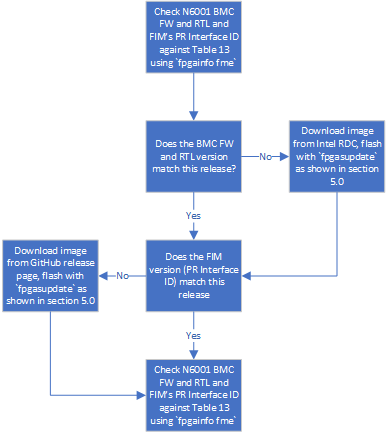
If your Intel® FPGA SmartNIC N6001-PL does not have the 2022.3.1 version of the FIM and BMC, use this section to begin your upgrade process. The upgrade process depends on both the OPAE SDK and kernel drivers, which were installed in sections 3.0 Intel OFS DFL Kernel Drivers and 4.0 OPAE Software Development Kit. Use the output of fpgainfo and compare against the table below to determine if an upgade is necessary.
Table 17: FIM Version Summary for Intel OFS 2023.1 Release
| FIM Version | Bitstream ID | Pr Interface ID | File Name | Download Location |
|---|---|---|---|---|
| 1 | 360571655605884772 | d8fd88a7-8683-57ba-8be6-a1e058b7d4ed | ofs_top_page[1 / 2]_unsigned_user[1 / 2].bin | ofs-2023.1 Release Page |
Table 18: BMC Version Summary for Intel OFS 2023.1 Release
| BMC FW and RTL Version | File Name | Download Location |
|---|---|---|
| 3.14.0 | AC_BMC_RSU_user_retail_3.14.0_unsigned.rsu | n/a |
Sample output of fpgainfo with matching values:
Intel Acceleration Development Platform N6001
Board Management Controller NIOS FW version: 3.14.0
Board Management Controller Build version: 3.14.0
//****** FME ******//
Object Id                        : 0xED00001
PCIe s:b:d.f                     : 0000:B1:00.0
Vendor Id                        : 0x8086
Device Id                        : 0xBCCE
SubVendor Id                     : 0x8086
SubDevice Id                     : 0x1771
Socket Id                        : 0x00
Ports Num                        : 01
Bitstream Id                     : 360571655605884772
Bitstream Version                : 5.0.1
Pr Interface Id                  : d8fd88a7-8683-57ba-8be6-a1e058b7d4ed
Boot Page                        : user1
Factory Image Info               : a2b5fd0e7afca4ee6d7048f926e75ac2
User1 Image Info                 : d8fd88a7-8683-57ba-8be6-a1e058b7d4ed
User2 Image Info                 : d8fd88a7-8683-57ba-8be6-a1e058b7d4ed
- If your output does not match the table above, download the appropriate FIM image from the Intel OFS 2023.1 (Intel Agilex) release page. Once downloaded transfer the file over to the server and use the fpgasupdate utility to perform an upgrade of the BMC.
$ sudo fpgasupdate AC_BMC_RSU_user_retail_3.14.0_unsigned.rsu
[2022-04-14 16:32:47.93] [WARNING ] Update starting. Please do not interrupt.
[2022-04-14 16:32:47.93] [INFO    ] updating from file /home/user/AC_BMC_RSU_user_retail_3.14.0_unsigned.rsu with size 904064
[2022-04-14 16:32:47.94] [INFO    ] waiting for idle
[2022-04-14 16:32:47.94] [INFO    ] preparing image file
[2022-04-14 16:33:26.98] [INFO    ] writing image file
(100%) [████████████████████] [904064/904064 bytes][Elapsed Time: 0:00:00.00]
[2022-04-14 16:33:26.98] [INFO    ] programming image file
(100%) [████████████████████] [Elapsed Time: 0:00:26.02]
[2022-04-14 16:33:53.01] [INFO    ] update of 0000:b1:00.0 complete
[2022-04-14 16:33:53.01] [INFO    ] Secure update OK
[2022-04-14 16:33:53.01] [INFO    ] Total time: 0:01:05.07
sudo rsu bmcimg
```bash
$ sudo fpgasupdate ofs_top_page1_unsigned_user1.bin <PCI ADDRESS>
[2022-04-14 16:42:31.58] [WARNING ] Update starting. Please do not interrupt.
[2022-04-14 16:42:31.58] [INFO    ] updating from file ofs_top_page1_pacsign_user1.bin with size 19928064
[2022-04-14 16:42:31.60] [INFO    ] waiting for idle
[2022-04-14 16:42:31.60] [INFO    ] preparing image file
[2022-04-14 16:42:38.61] [INFO    ] writing image file
(100%) [████████████████████] [19928064/19928064 bytes][Elapsed Time: 0:00:16.01]
[2022-04-14 16:42:54.63] [INFO    ] programming image file
(100%) [████████████████████][Elapsed Time: 0:06:16.40]
[2022-04-14 16:49:11.03] [INFO    ] update of 0000:b1:00.0 complete
[2022-04-14 16:49:11.03] [INFO    ] Secure update OK
[2022-04-14 16:49:11.03] [INFO    ] Total time: 0:06:39.45
sudo rsu fpga --page=user1 <PCI ADDRESS>
```
- Verify output of fpgainfo matches the table above.
Notices & Disclaimers
Intel® technologies may require enabled hardware, software or service activation. No product or component can be absolutely secure. Performance varies by use, configuration and other factors. Your costs and results may vary. You may not use or facilitate the use of this document in connection with any infringement or other legal analysis concerning Intel products described herein. You agree to grant Intel a non-exclusive, royalty-free license to any patent claim thereafter drafted which includes subject matter disclosed herein. No license (express or implied, by estoppel or otherwise) to any intellectual property rights is granted by this document, with the sole exception that you may publish an unmodified copy. You may create software implementations based on this document and in compliance with the foregoing that are intended to execute on the Intel product(s) referenced in this document. No rights are granted to create modifications or derivatives of this document. The products described may contain design defects or errors known as errata which may cause the product to deviate from published specifications. Current characterized errata are available on request. Intel disclaims all express and implied warranties, including without limitation, the implied warranties of merchantability, fitness for a particular purpose, and non-infringement, as well as any warranty arising from course of performance, course of dealing, or usage in trade. You are responsible for safety of the overall system, including compliance with applicable safety-related requirements or standards. © Intel Corporation. Intel, the Intel logo, and other Intel marks are trademarks of Intel Corporation or its subsidiaries. Other names and brands may be claimed as the property of others.
OpenCL and the OpenCL logo are trademarks of Apple Inc. used by permission of the Khronos Group™.