Board Installation Guidelines: Intel Agilex® 7 FPGA F-Series Development Kit (2x F-Tile) and Intel Agilex® 7 FPGA I-Series Development Kit (2x R-Tile and 1xF-Tile)
Last updated: December 10, 2024
1.0 Introduction
1.1 About This Document
The purpose of this document is to educate users of the following acceleration platforms on board installation and server environment setup for the F-Series (2x F-Tile) and I-Series (2x R-Tile and 1xF-Tile) Development Kits. After reading the document a user shall be able to:
- Safely install and remove a development kit
- Set up their server BIOS with the recommended settings
- Learn about thermal cooling requirements for their platform
This document will include notes where board installation or information differs between platforms. If no such note exists, you may assume it is applicable to both platforms.
1.2 Audience
The information in this document is intended for customers evaluating the PCIe Attach shell on supported development kit platforms. This reference is a starting point for evaluation and development of the OFS compliant shell designs and workloads. This document will not cover software installation or platform validation, as those are shown in their respective documents.
Note: Code command blocks are used throughout the document. Full command output may not be shown for the sake of brevity.
Table 1: Terminology
| Term | Abbreviation | Description |
|---|---|---|
| Advanced Error Reporting | AER | The PCIe AER driver is the extended PCI Express error reporting capability providing more robust error reporting. (link) |
| Accelerator Functional Unit | AFU | Hardware Accelerator implemented in FPGA logic which offloads a computational operation for an application from the CPU to improve performance. Note: An AFU region is the part of the design where an AFU may reside. This AFU may or may not be a partial reconfiguration region. |
| Basic Building Block | BBB | Features within an AFU or part of an FPGA interface that can be reused across designs. These building blocks do not have stringent interface requirements like the FIM's AFU and host interface requires. All BBBs must have a (globally unique identifier) GUID. |
| Best Known Configuration | BKC | The software and hardware configuration Intel uses to verify the solution. |
| Board Management Controller | BMC | Supports features such as board power managment, flash management, configuration management, and board telemetry monitoring and protection. The majority of the BMC logic is in a separate component, such as an Intel® Max® 10 or Intel Cyclone® 10 device; a small portion of the BMC known as the PMCI resides in the main Agilex FPGA. |
| Configuration and Status Register | CSR | The generic name for a register space which is accessed in order to interface with the module it resides in (e.g. AFU, BMC, various sub-systems and modules). |
| Data Parallel C++ | DPC++ | DPC++ is Intel’s implementation of the SYCL standard. It supports additional attributes and language extensions which ensure DCP++ (SYCL) is efficiently implanted on Intel hardware. |
| Device Feature List | DFL | The DFL, which is implemented in RTL, consists of a self-describing data structure in PCI BAR space that allows the DFL driver to automatically load the drivers required for a given FPGA configuration. This concept is the foundation for the OFS software framework. (link) |
| FPGA Interface Manager | FIM | Provides platform management, functionality, clocks, resets and standard interfaces to host and AFUs. The FIM resides in the static region of the FPGA and contains the FPGA Management Engine (FME) and I/O ring. |
| FPGA Management Engine | FME | Performs reconfiguration and other FPGA management functions. Each FPGA device only has one FME which is accessed through PF0. |
| Host Exerciser Module | HEM | Host exercisers are used to exercise and characterize the various host-FPGA interactions, including Memory Mapped Input/Output (MMIO), data transfer from host to FPGA, PR, host to FPGA memory, etc. |
| Input/Output Control | IOCTL | System calls used to manipulate underlying device parameters of special files. |
| Intel Virtualization Technology for Directed I/O | Intel VT-d | Extension of the VT-x and VT-I processor virtualization technologies which adds new support for I/O device virtualization. |
| Joint Test Action Group | JTAG | Refers to the IEEE 1149.1 JTAG standard; Another FPGA configuration methodology. |
| Memory Mapped Input/Output | MMIO | The memory space users may map and access both control registers and system memory buffers with accelerators. |
| oneAPI Accelerator Support Package | oneAPI-asp | A collection of hardware and software components that enable oneAPI kernel to communicate with oneAPI runtime and OFS shell components. oneAPI ASP hardware components and oneAPI kernel form the AFU region of a oneAPI system in OFS. |
| Open FPGA Stack | OFS | OFS is a software and hardware infrastructure providing an efficient approach to develop a custom FPGA-based platform or workload using an Intel, 3rd party, or custom board. |
| Open Programmable Acceleration Engine Software Development Kit | OPAE SDK | The OPAE SDK is a software framework for managing and accessing programmable accelerators (FPGAs). It consists of a collection of libraries and tools to facilitate the development of software applications and accelerators. The OPAE SDK resides exclusively in user-space. |
| Platform Interface Manager | PIM | An interface manager that comprises two components: a configurable platform specific interface for board developers and a collection of shims that AFU developers can use to handle clock crossing, response sorting, buffering and different protocols. |
| Platform Management Controller Interface | PMCI | The portion of the BMC that resides in the Agilex FPGA and allows the FPGA to communicate with the primary BMC component on the board. |
| Partial Reconfiguration | PR | The ability to dynamically reconfigure a portion of an FPGA while the remaining FPGA design continues to function. For OFS designs, the PR region is referred to as the pr_slot. |
| Port | N/A | When used in the context of the fpgainfo port command it represents the interfaces between the static FPGA fabric and the PR region containing the AFU. |
| Remote System Update | RSU | The process by which the host can remotely update images stored in flash through PCIe. This is done with the OPAE software command "fpgasupdate". |
| Secure Device Manager | SDM | The SDM is the point of entry to the FPGA for JTAG commands and interfaces, as well as for device configuration data (from flash, SD card, or through PCI Express* hard IP). |
| Static Region | SR | The portion of the FPGA design that cannot be dynamically reconfigured during run-time. |
| Single-Root Input-Output Virtualization | SR-IOV | Allows the isolation of PCI Express resources for manageability and performance. |
| SYCL | SYCL | SYCL (pronounced "sickle") is a royalty-free, cross-platform abstraction layer that enables code for heterogeneous and offload processors to be written using modern ISO C++ (at least C++ 17). It provides several features that make it well-suited for programming heterogeneous systems, allowing the same code to be used for CPUs, GPUs, FPGAs or any other hardware accelerator. SYCL was developed by the Khronos Group, a non-profit organization that develops open standards (including OpenCL) for graphics, compute, vision, and multimedia. SYCL is being used by a growing number of developers in a variety of industries, including automotive, aerospace, and consumer electronics. |
| Test Bench | TB | Testbench or Verification Environment is used to check the functional correctness of the Design Under Test (DUT) by generating and driving a predefined input sequence to a design, capturing the design output and comparing with-respect-to expected output. |
| Universal Verification Methodology | UVM | A modular, reusable, and scalable testbench structure via an API framework. In the context of OFS, the UVM enviroment provides a system level simulation environment for your design. |
| Virtual Function Input/Output | VFIO | An Input-Output Memory Management Unit (IOMMU)/device agnostic framework for exposing direct device access to userspace. (link) |
1.3 Required Hardware for Installation
Table 2: Hardware BKC for OFS PCIe Attach targeting the F-Series Development Kit
The following table highlights the hardware which composes the Best Known Configuation (BKC) for the OFS 2024.1-1 PCIe Attach release targeting F-Series Development Kit.
Note: The Dell R750 server product line is known not to work with this release.
| Component | Link |
|---|---|
| Agilex® 7 FPGA F-Series Development Kit (2x F-Tile) | https://www.intel.com/content/www/us/en/products/details/fpga/development-kits/agilex/agf027-and-agf023.html |
| Intel FPGA Download Cable II (optional) | https://www.intel.com/content/www/us/en/products/sku/215664/intel-fpga-download-cable-ii/specifications.html |
| SuperMicro SYS-220HE-FTNR | https://www.supermicro.com/en/products/system/hyper/2u/sys-220he-ftnr |
In addition to the above, both OFS enabled development kit platforms require either an auxillary power cable for the 12 V-Auxiliary 2x4 PCIe* power connector, or the standalone AC Power Supply with associated 2x4 power connector. You must choose one of these modes to operate your device in.
A server ATX power cable will differ between vendors - review the pinout of the power connector on the Intel Agilex® 7 FPGA I-Series Development Kit User Guide or Intel Agilex® 7 F-Series FPGA (Two F-Tiles) Development Kit User Guide as a reference for ordering. Although this is not always the case, often the standard 2x4 PCIe power connector that is required to enable a GPU in your server will also work for an FPGA-based development kit.
In addition, the server used to house either dev kit must meet the following guidelines:
- The server platform must be able to fit, power, and cool an F-Series Dev Kit or I-Series Dev Kit as described in their mechanical details
- The server should be able to run PCIe at Gen 4.0 speeds to properly test designs and demos
Both platforms ship with an embedded Intel® FPGA Download Cable II on the rear of the device which will be used for device programming. An on-board micro-USB connector on the rear of the development kit provides the data to the Intel® MAX® 10. This allows configuration of the FPGA using a USB cable directly connected to a PC running the Intel® Quartus® Prime software without requiring the external download cable dongle. An external download cable dongle can also be used on J10 to configure the FPGA, although both cannot be used at the same time.
2.0 Server Settings
2.1 BIOS Settings
These are the host BIOS settings known to work with the either dev kit. Information about the server's currently loaded firmware and BIOS settings can be found through its remote access controller, or by manually entering the BIOS by hitting a specific key during power on. Your specific server platform will include instructions on proper BIOS configuration and should be followed when altering settings.
- PCIe slot width must be set to x16
- PCIe slot speed must be set to 4
- PCIe slot must have iommu enabled
- Intel VT for Directed I/O (VT-d) must be enabled
2.2 Server Fan Speed
The recommended fan speed setting is to use the 100% preset. If using a different server model, refer to that server’s user guide for instructions on changing fan speed. The following steps will help users on the SuperMicro platform.
- Log in to the SuperMicro server BMC. (This requires an Ethernet cable to be attached to an open port on the server labelled “IPMI”.)
- During boot the BMC’s login IP will be presented on the screen. Open this IP address in a browser and enter your login credentials. The default username is ADMIN, and the default password has been printed on the service tag that pulls out from the front of the server case.
- On the left menu select System -> Component Info, select the Fan tab, under Advanced Settings click the circle next to Full Speed.
3.0 Development Kit Installation
3.1 Preparing the F-Series Development Kit for Installation into a Server
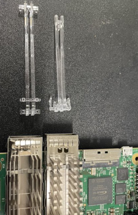
Light pipes located on the top of the QSFP cages for the F-Series Dev Kit may or may not cause physical fit issues for some server platforms. If you run into any issues during installation you may remove the light pipes:
-
The DK-DEV-AGF027F1ES (or it is called the F - tile Dev Kit, or FM86 Dev Kit) has LED light pipes on top of the QSFP cages.
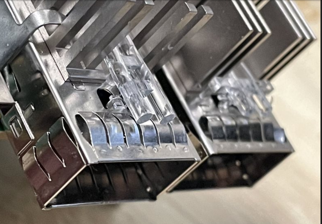
These light pipes interfere with the server PCIe slot faceplate.
-
The light pipes can be easily removed by prying them off using a small screwdriver for leverage, then pushing the light pipes back to remove the retaining clips from the QSFP cage.
3.2 Default Switch Settings
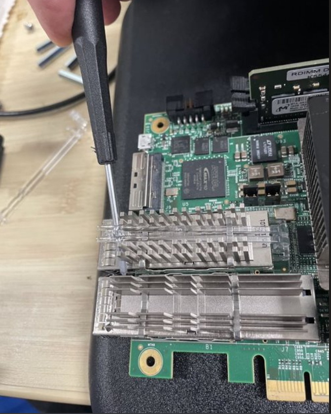
Double check that your development kit switch settings match those listed as the default positions in the user guide prior to installation. An F Tile Dev Kit is used as an example in this section.
-
Board switch definitions can be found in the Intel Agilex® 7 F-Series FPGA (Two F-Tiles) Development Kit User Guide or Intel Agilex® 7 FPGA I-Series Development Kit User Guide.
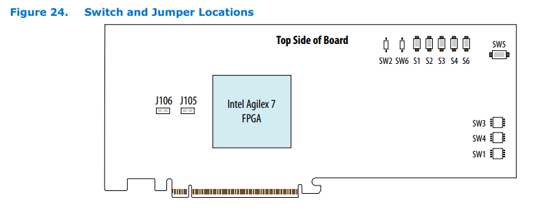
See the image below for SW1, SW4 and SW3.
Before inserting into a server, set SW5 to 'ON'.
-
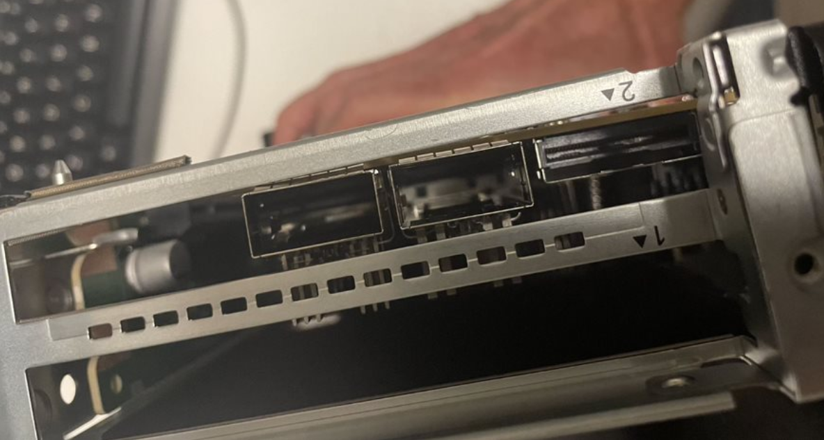
Below shows an F-Series Dev Kit installed into a PCIe riser with the light pipes removed.
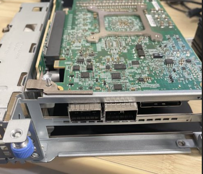
3.3 Physical Installation Procedure
The following instructions will help ensure safe installation of the Intel Agilex® 7 FPGA F-Series Development Kit (2x F-Tile) and Intel Agilex® 7 FPGA I-Series Development Kit (2x R-Tile and 1xF-Tile) into a supported server platform. Safety and Regulatory information can be found under the product page for either development kit. It is assumed you have previously removed the light pipes mounted above the F-Series Dev Kit's QSFP cages before attempting to slot into a server mounted riser if they are an issue.
- Position the board over the selected connector on the motherboard
- Press down gently and firmly seat the card in a PCIe slot. Depending on the server model being used, you may need to secure a retention screw or rotate retention clips over the development kit's faceplate.
- Do not bend the card while inserting in a slot. Do not apply too much pressure while inserting.
- Plug a standard 2x4 auxiliary power cord available from the server's ATX power supply or from the riser itself to the respective matching power connected on the board (J11). Both the PCIe slot and auxiliary PCIe power cable are required to power the entire board.
3.4 JTAG Setup
Both Development Kits have an on-board FPGA Download Cable II module which is used to program the FPGA via JTAG. Perform the following steps to establish a JTAG connection:
Pre-requisites:
- This walkthrough requires an OFS Agilex PCIe Attach deployment environment. Refer to the Software Installation Guide: PCIe Attach for instructions on setting up a deployment environment.
- This walkthrough requires a workstation with Quartus Prime Pro Version 23.4 tools installed, specifically the
jtagconfigtool.
Steps:
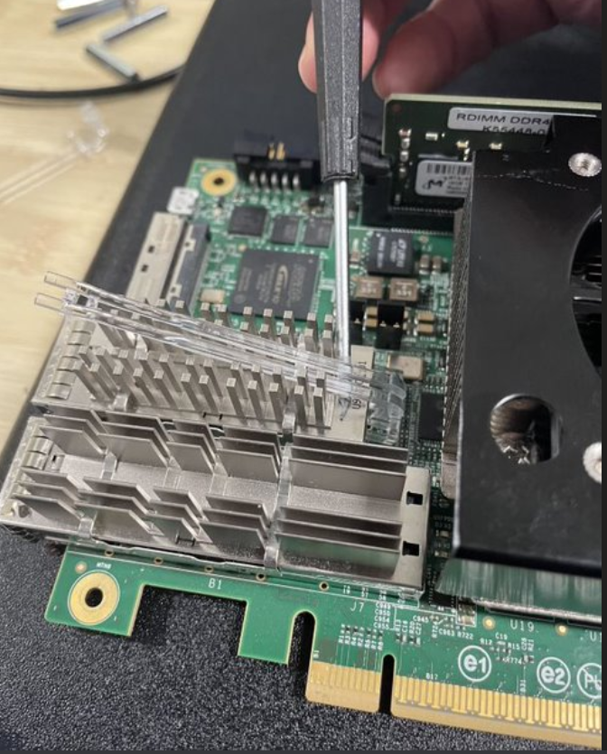
-
Refer to the following figure for Steps 2 and 3.
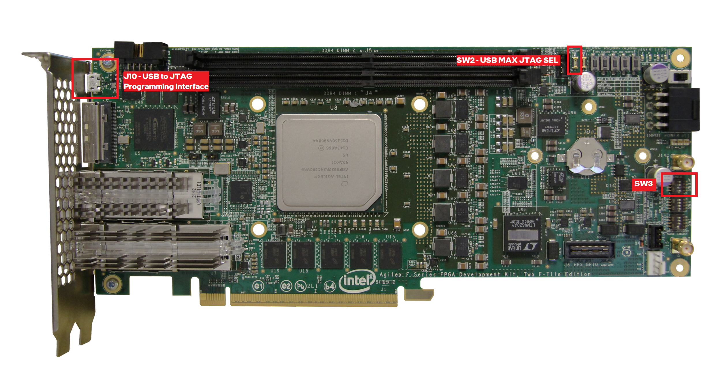
-
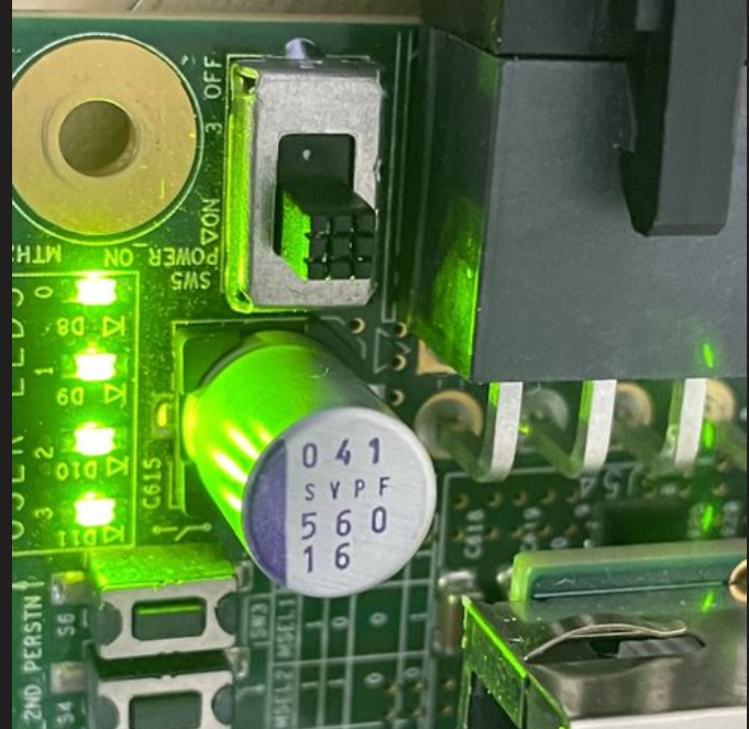
Locate Single DIP Switch SW2 and 4-position DIP switch SW3 on the fseries-dk. These switches control the JTAG setup for the board. Ensure that both SW2 and SW3.3 are set to
ON. -
Locate the J10 Micro-USB port on the fseries-dk. Connect a Micro-USB to USB-A cable between the J10 port and the workstation that has Quartus Prime Pro tools installed.
-
Use the
jtagconfigtool to check that the JTAG chain contains the AGFB027R24C2E2VR2 device.Example expected output:
This concludes the walkthrough for establishing a JTAG connection on the fseries-dk.