UVM Simulation User Guide: OFS for Intel® Agilex® PCIe Attach
| Term | Abbreviation | Description |
|---|---|---|
| Advanced Error Reporting | AER | The PCIe AER driver is the extended PCI Express error reporting capability providing more robust error reporting. (link) |
| Accelerator Functional Unit | AFU | Hardware Accelerator implemented in FPGA logic which offloads a computational operation for an application from the CPU to improve performance. Note: An AFU region is the part of the design where an AFU may reside. This AFU may or may not be a partial reconfiguration region. |
| Basic Building Block | BBB | Features within an AFU or part of an FPGA interface that can be reused across designs. These building blocks do not have stringent interface requirements like the FIM's AFU and host interface requires. All BBBs must have a (globally unique identifier) GUID. |
| Best Known Configuration | BKC | The software and hardware configuration Intel uses to verify the solution. |
| Board Management Controller | BMC | Supports features such as board power managment, flash management, configuration management, and board telemetry monitoring and protection. The majority of the BMC logic is in a separate component, such as an Intel Max10 or Intel Cyclone10 device; a small portion of the BMC known as the PMCI resides in the main Agilex FPGA. |
| Configuration and Status Register | CSR | The generic name for a register space which is accessed in order to interface with the module it resides in (e.g. AFU, BMC, various sub-systems and modules). |
| Data Parallel C++ | DPC++ | DPC++ is Intel’s implementation of the SYCL standard. It supports additional attributes and language extensions which ensure DCP++ (SYCL) is efficiently implemented on Intel hardware. |
| Device Feature List | DFL | The DFL, which is implemented in RTL, consists of a self-describing data structure in PCI BAR space that allows the DFL driver to automatically load the drivers required for a given FPGA configuration. This concept is the foundation for the OFS software framework. (link) |
| FPGA Interface Manager | FIM | Provides platform management, functionality, clocks, resets and standard interfaces to host and AFUs. The FIM resides in the static region of the FPGA and contains the FPGA Management Engine (FME) and I/O ring. |
| FPGA Management Engine | FME | Performs reconfiguration and other FPGA management functions. Each FPGA device only has one FME which is accessed through PF0. |
| Host Exerciser Module | HEM | Host exercisers are used to exercise and characterize the various host-FPGA interactions, including Memory Mapped Input/Output (MMIO), data transfer from host to FPGA, PR, host to FPGA memory, etc. |
| Input/Output Control | IOCTL | System calls used to manipulate underlying device parameters of special files. |
| Intel Virtualization Technology for Directed I/O | Intel VT-d | Extension of the VT-x and VT-I processor virtualization technologies which adds new support for I/O device virtualization. |
| Joint Test Action Group | JTAG | Refers to the IEEE 1149.1 JTAG standard; Another FPGA configuration methodology. |
| Management Component Transport Protocol | MCTP | A standardized model for communication with management controllers. Defines the transport protocol carrying PLDM messages through the BMC. |
| Memory Mapped Input/Output | MMIO | The memory space users may map and access both control registers and system memory buffers with accelerators. |
| oneAPI Accelerator Support Package | oneAPI-asp | A collection of hardware and software components that enable oneAPI kernel to communicate with oneAPI runtime and OFS shell components. oneAPI ASP hardware components and oneAPI kernel form the AFU region of a oneAPI system in OFS. |
| Open FPGA Stack | OFS | OFS is a software and hardware infrastructure providing an efficient approach to develop a custom FPGA-based platform or workload using an Intel, 3rd party, or custom board. |
| Open Programmable Acceleration Engine Software Development Kit | OPAE-SDK | The OPAE-SDK is a software framework for managing and accessing programmable accelerators (FPGAs). It consists of a collection of libraries and tools to facilitate the development of software applications and accelerators. The OPAE SDK resides exclusively in user-space. |
| Platform Interface Manager | PIM | An interface manager that comprises two components: a configurable platform specific interface for board developers and a collection of shims that AFU developers can use to handle clock crossing, response sorting, buffering and different protocols. |
| Platform Level Data Model | PLDM | A specification for reporting telemetry data to the host, such as board temperature, voltage, and current. |
| Platform Management Controller Interface | PMCI | The portion of the BMC that resides in the Agilex FPGA and allows the FPGA to communicate with the primary BMC component on the board. |
| Partial Reconfiguration | PR | The ability to dynamically reconfigure a portion of an FPGA while the remaining FPGA design continues to function. For OFS designs, the PR region is referred to as the pr_slot. |
| Port | N/A | When used in the context of the fpgainfo port command it represents the interfaces between the static FPGA fabric and the PR region containing the AFU. |
| Remote System Update | RSU | The process by which the host can remotely update images stored in flash through PCIe. This is done with the OPAE software command "fpgasupdate". |
| Secure Device Manager | SDM | The SDM is the point of entry to the FPGA for JTAG commands and interfaces, as well as for device configuration data (from flash, SD card, or through PCI Express* hard IP). |
| Static Region | SR | The portion of the FPGA design that cannot be dynamically reconfigured during run-time. |
| Single-Root Input-Output Virtualization | SR-IOV | Allows the isolation of PCI Express resources for manageability and performance. |
| SYCL | SYCL | SYCL (pronounced "sickle") is a royalty-free, cross-platform abstraction layer that enables code for heterogeneous and offload processors to be written using modern ISO C++ (at least C++ 17). It provides several features that make it well-suited for programming heterogeneous systems, allowing the same code to be used for CPUs, GPUs, FPGAs or any other hardware accelerator. SYCL was developed by the Khronos Group, a non-profit organization that develops open standards (including OpenCL) for graphics, compute, vision, and multimedia. SYCL is being used by a growing number of developers in a variety of industries, including automotive, aerospace, and consumer electronics. |
| Test Bench | TB | Testbench or Verification Environment is used to check the functional correctness of the Design Under Test (DUT) by generating and driving a predefined input sequence to a design, capturing the design output and comparing with-respect-to expected output. |
| Universal Verification Methodology | UVM | A modular, reusable, and scalable testbench structure via an API framework. In the context of OFS, the UVM enviroment provides a system level simulation environment for your design. |
| Virtual Function Input/Output | VFIO | An Input-Output Memory Management Unit (IOMMU)/device agnostic framework for exposing direct device access to userspace. (link) |
1 Overview
1.1 About this Document
This document serves as a set-up and user guide for the UVM simulation tool using Open FPGA Stack (OFS) for Agilex® 7 FPGAs PCIe Attach and the Agilex® 7 FPGA F-Series Development Kit (2x F-Tile). After reviewing the document, you will be able to:
- Set-up the UVM verification tool suite
- Run pre-existing UVM unit tests and also create new UVM tests for your design
NOTE:
This guide uses the Intel® FPGA SmartNIC N6001-PL as the platform for all example steps. Additionally, this guide and the example steps can be used with other platforms, such as the Agilex® 7 FPGA F-Series Development Kit (2x F-Tile).
2 Introduction to UVM
The Functional Verification Environment for OFS is UVM (Universal Verification Methodology) compliant and provides configurable setup for verifying various FIM features in simulation.
The purpose of this document is to demonstrate a full chip level and unit level UVM based verification environment for the current base shell FIM architecture as well as providing examples to extend the setup for different OFS variants by reusing the existing architecture and infrastructure for UVM based verification.
3 Universal Testbench Architecture
3.1 Overview
The main idea behind UVM is to develop modular, reusable, and a scalable testbench structure by providing an API framework that can be deployed across multiple projects.
3.2 Core Verification Concepts
The following is the list of verification components that will be used to design a UVM testbench architecture:
• Sequencer
• Driver
• Monitor
• Scoreboard
• Virtual Sequencer
• Interface
• Verification Environment
• TOP Testbench
Figure 1 provides the general UVM Testbench and the verification components involved in the top-level architecture.
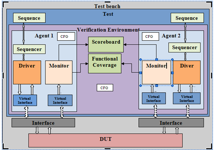
Figure 1 Typical UVM Testbench
4 OFS Testbench Architecture
4.1 Overview
OFS (Open FPGA Stack) provides a UVM (Universal Verification Methodology) environment for the FIM with a modular, reusable, and scalable testbench structure via an API framework.
The framework consists of a FIM Testbench which is UVM compliant and integrates third party VIPs from Synopsys for PCI Express, Arm® AMBA® 4 AXI4Arm® AMBA® 4 AXI4-Streaming interface and Arm® AMBA® 4 AXI4-Memory Mapped interface for comprehensive verification. The user will need to acquire licenses for these VIPs to use this Testbench. UVM RAL(Register Abstraction Level) is used for CSR (Command and Status Registers) verification.
The qualified verification IPs will help to detect incorrect protocol behavior, help to focus on FIM features and accelerate the verification process.
Verification components include:
• FIM monitor to detect correct design behavior
• FIM assertions for signal level integrity testing
• Arm AMBA Arm® AMBA® 4 AXI4 scoreboards to check data integrity
• FIM coverage to collect functional data
4.2 Base FIM DUT
The hardware architecture of an Agilex FIM is based on the OFS hardware architecture. The following is the list of features and subsystems supported in the base shell.
•   PCIe Subsystem
•   HSSI Subsystem
•   Memory Subsystem
•   HPS Subsystem
•   FME
•   AFU with PR support
•   QSFP Controllers
•   PMCI Controller, MCTP
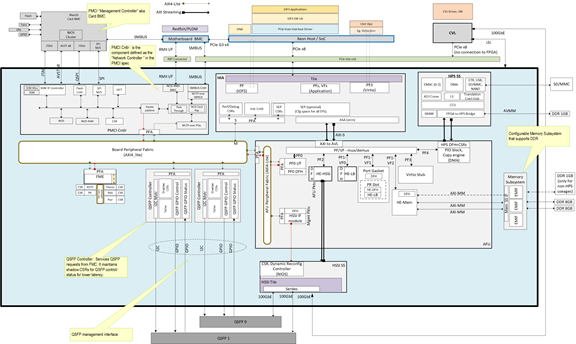
Figure 2 DUT Base Shell Diagram
Figure 2 shows the high level architecture of an Agilex Base Shell. It has a Gen4x16, 100G Ethernet Datapath in a 2x4x25G configuration. The Agilex Base Shell is a shell that will enable a user to build other shell variants for a custom configuration. For the N6001 board there is one shell variant
base_x16
4.3 Full Chip Level Verification Archiecture for FIM
Figure 3 shows a graphical representation a full chip testbench that includes major RTL blocks depicted in a OFS Agilex based UVM environment
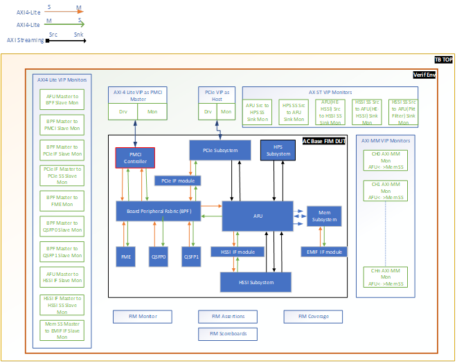
Figure 3 OFS FIM Testbench
The major connection is the interface between the Xeon CPU and the FPGA where the PCIe Verification IP is connected to PCIe Subsystem. Therefore, as a full chip simulation environment, PCIe host VIP is the sole VIP/BFM used. PCIe host VIP connects to PCIe device which resides in FPGA in serial mode.
4.3.1 Testbench components
4.3.1.1 TB TOP
TOP is the top level testbench and consists of a FIM DUT instance and top-level UVM Verification Environment instance. It binds RTL inputs with the verification environmnet interfaces to drive stimulus. It also has clock generation and reset driving logic.
4.3.1.2 FIM Verification Environment
This is the top most verification environment class and consists of the protocol specific PCI Express and AXI UVM environment VIP instances, Monitors, Scoreboards, Assertions, Functional coverage Modules and other verification components. It instantiates Virtual sequencers to control stimuli for FIM traffic from different sequencers of the VIPs.
4.3.1.3 Synopsys VIPs
4.3.1.3.1 PCI VIP as Host
This is Synopsys Licensed PCI Express Gen4 VIP and acts as Root Port. The PCI Express link is connected to the DUT using TX-RX lanes. Agent is an active component and includes a sequencer to generate TLPs, Driver to drive it on a PCI Express link and Monitor to check the protocol correctness.
4.3.1.3.2 AXI-Streaming VIP Monitors
This is Synopsys Licensed AXI streaming interface Verification IP used as a Passive Agent to monitor AXI-ST links at various points. Please refer to Figure 3 to see all the AXI-ST monitors connected to different modules.
4.3.1.3.3 AXI4-Memory Mapped VIP Monitors
This is Synopsys Licensed Arm® AMBA® 4 AXI4 memory mapped interface Verification IP used in passive mode to observe memory requests. For each master-slave pair, the verification environment has a VIP instantiated in passive mode for monitoring protocol violations and performing data integrity checks.
4.3.1.3.4 AXI4-Lite VIP Monitors
This is Synopsys Licensed Arm® AMBA® 4 AXI4 Lite interface Verification IP used in passive mode to observe MMIO requests. For each master-slave pair, the verification environment has a VIP instantiated in passive mode for monitoring protocol violations and perfoming data integrity checks. Please refer to Figure 3 to see all the Arm® AMBA® 4 AXI4-Lite monitors connected to different modules.
4.3.1.3.5 AXI4-Lite VIP as PMCI Master
This is Synopsys Licensed Arm® AMBA® 4 AXI4 Lite interface Verification IP used to drive and observe MMIO requests as PMCI master. For each master-slave pair, the verification environment has a VIP instantiated in active mode and includes a sequencer to generate MMIO requests, driver to drive these requests on AXI-4 Lite interface to BPF and a monitor for observing protocol violations and data integrity checks.
4.3.1.4 AXI4-S Scoreboard
The Arm® AMBA® 4 AXI4-S scoreboard checks data integrity of source and sink components. It has input transactions from VIP monitors and a TLP to AXI converter for PCIe TLP packets. It makes sure the valid TLPs or AXI transactions are not missed while traversing from Host to AFU and reverse. The scoreboard will be disabled for error testing especially for invalid TLP requests and UR responses.
4.3.1.5 Virtual Sequencer
The virtual sequencer is the top-level sequencer which controls Enumeration, MMIO Requests, downstream and Upstream traffic as well as HSSI and Memory transactions. It makes sure that the transactions are ordered correctly as per the design specification while running a UVM test simulation.
4.3.1.6 FIM Monitor
The FIM monitor is used for checking the correctness of a specific FIM feature. As an example, a user can add interrupt related checks, error generation and clearing checks, Protocol checker impacts etc. in this component.
This would be an independent plug-n-play component and can be reused with any user developed UVM FIM TB.
4.3.1.7 FIM Assertions
The assertion component is used for checking the signal level integrity of a specific FIM feature or behavior. As an example, we can add interrupt signal triggering and clear assertions, Error detection to error register bit assertions, protocol checker and clearing logic, FLR behavior assertion etc. in this top-level module. There are alos assertions to make sure the inputs are driven correctly to catch errors in a users simulation.
This would be an independent plug-n-play component and can be reused with any user developed UVM FIM TB.
4.3.1.8 FIM Functional Coverage
The FIM functional coverage component will have the functional coverage of each feature like interrupts, CSR's, MMIO requests, Byte align transactions, error reporting etc. to demonstrate a variety of FIM features. This will help us to find holes in the design as well as wide verification coverage to make sure thorough testing of a design. It will also provide a user what the FIM is capable of and how much code coverage they are testing.
This would be an independent plug-n-play component and can be reused with any user developed UVM FIM TB.
5 UVM Verification set-up
To run the tutorial steps in this guide requires the following development environment:
| Item | Version |
|---|---|
| Intel Quartus Prime Pro | Intel Quartus Prime Pro 23.4 |
| Simulator | Synopsys VCS S-2021.09-SP1 or newer for UVM simulation of top level FIM |
| Simulator (Questasim) | Questasim 2023.4 or newer for UVM simulation of top level FIM |
5.1 UVM Prerequisite
Retrieve OFS repositories.
The OFS FIM source code is included in the OTCShare GitHub repository. Create a new directory to use as a clean starting point to store the retrieved files. The following is a short description of each repository, followed by the git commands for cloning. The instructions section uses the HTTPS git method for cloning repositories. Cloning the repo using the HTTPS method requires a personal access token. Please see this blog post for information about obtaining a personal access token Token authentication requirements for Git operations.
Navigate to location for storage of OFS source, create the top-level source directory and clone OFS repositories.
$ mkdir ofs-2024.1-1
$ cd ofs-2024.1-1
$ export OFS_BUILD_ROOT=$PWD
$ git clone --recurse-submodules https://github.com/OFS/ofs-agx7-pcie-attach.git

Cloning into 'ofs-agx7-pcie-attach'...'
Username for 'https://github.com': <<Enter your git hub username>>
Password for 'https://<<Your username>>': <<Enter your personal access token>>
remote: Enumerating objects:  ....
...
...
Resolving deltas  ..., done.

$ cd ofs-agx7-pcie-attach
$ git checkout tags/ofs-2024.1-1
Verify that the correct tag/branch have been checked out
$ git describe --tags

$ ofs-2024.1-1
5.2 License Requirements
The FIM Testbench is UVM compliant and integrates third party VIP's from Synopsys for PCI Express, Arm® AMBA® 4 AXI4Arm® AMBA® 4 AXI4-Streaming interface and Arm® AMBA® 4 AXI4-Memory Mapped interface for comprehensive verification. The user will need to acquire licenses for these VIPs to use this TB. UVM RAL (Register Abstraction Layer) is used for CSR Verification.
The Qualified Verification IPs will help to detect incorrect protocol behavior easily, help to focus on FIM features and accelerate the verification process.
• VCS & DVE
• SNPS-Assertions
• Verdi
• VerdiCoverage
• VerdiSimDB
• VerdiTransactionDebugUltra
• VIP-AMBA-AXI-SVT
• VIP-AMBA-STREAM-SVT
• VIP-PCIE-SVT
• VIP-PCIE-TS-SVT
• VIP-PCIE-G3-OPT-SVT
• VIP-Ethernet-SVT
5.3 Software Tools Requirements
The following tools are required for successful UVM set-up
- Python 3.6.8
- Synopsys PCIE and AMBA AXI UVM VIP Q-2020.03A License
- Synopsys Verdi R-2020.12-SP2 License
Note: Makefile can be modified to use DVE instead of Verdi
- VCS R-2020.12-SP2 License
5.4 Creating a Software Tools Script
The UVM tool set-up is best done by creating a simple set-up script so all applicable tools are sourced before running the tests.
The following environment variables can be pasted into a script and used prior to running the UVM verification environment
License Files
export LM_LICENSE_FILE=
export SNPSLMD_LICENSE_FILE=
The license environment variables LM_LICENSE_FILE and SNPSLMD_LICENSE_FILE can point to a server license on your system.
General Environment Variables
export IOFS_BUILD_ROOT=$PWD
export OFS_ROOTDIR=<user_path>/ofs-agx7-pcie-attach
export WORKDIR=$OFS_ROOTDIR
Quartus Tools
export QUARTUS_HOME=<user_path>/intelFPGA_pro/23.4/quartus
export QUARTUS_ROOTDIR=$QUARTUS_HOME
export QUARTUS_INSTALL_DIR=$QUARTUS_ROOTDIR
export QUARTUS_ROOTDIR_OVERRIDE=$QUARTUS_ROOTDIR
export IMPORT_IP_ROOTDIR=$QUARTUS_ROOTDIR/../ip
export QSYS_ROOTDIR=$QUARTUS_ROOTDIR/../qsys/bin
export PATH=$QUARTUS_HOME/bin:$QUARTUS_HOME/qsys/bin:$QUARTUS_HOME/sopc_builder/bin/:$PATH
Synopsys Verification Tools
export DESIGNWARE_HOME=<user_path>/synopsys/vip_common/vip_Q-2020.03A
export PATH=$DESIGNWARE_HOME/bin:$PATH
export UVM_HOME=<user_path>/synopsys/vcsmx/S-2021.09-SP1/linux64/rhel/etc/uvm
export VCS_HOME=<user_path>/synopsys/vcsmx/S-2021.09-SP1/linux64/rhel
export PATH=$VCS_HOME/bin:$PATH
export VERDIR=$OFS_ROOTDIR/verification
export VIPDIR=$VERDIR
QuestaSIM Verification Tools
export MTI_HOME=<user_path>/mentor/questasim/2023.4/linux64
export PATH=$MTI_HOME/linux_x86_64/:$MTI_HOME/bin/:$PATH
export QUESTA_HOME=$MTI_HOME
6 Running a UVM Simulation Test and Analysing Results
6.1 Simulation
The default simulator used in the simulation script is Synopsys VCS-MX. Users can refer to the options and adopt the options for other simulators. The script is a makefile that calls vlogan, vcs and simv for compilation, elaboration and simulation, respectively.
6.2 File Structure
After cloning the repo, the verification and ofs-common directories contain all UVM verification related files. The directory structure is shown in Figure 4 below.

Figure 4 UVM Verification Directory File Structure
ofs-agx7-pcie-attach/verification/testbench has a testbench, uvm env, virtual sequencer, RAL etc.
ofs-agx7-pcie-attach/tests contains all uvm tests and sequences.
Users can run the simulation under "ofs-agx7-pcie-attach/verification/scripts" directory and the simulation result is outputted to a "sim" directory for Synopsys VCS or sim_msim for Questasim.
The simulation result folder is named after the test name with increasing suffix number. If user runs the same test multiple times, the suffix is incremented by 1 each time.
6.3 UVM Test Suite
The UVM environment contains a variety of tests that have been developed to test out the FIM portion of OFS.
The table below has four columns which describe the "Test Name", "DUT Scope", "Test Scenario" and the "Checking Criteria".
Tests are located at ofs-agx7-pcie-attach/verification/tests
| Test Name | DUT Scope | Test Scenario | Checking Criteria |
|---|---|---|---|
| afu_mmio_flr_pf0_test | PF0 FLR Reset | Apply FLR Reset for PF0 and deassert. Initiate MMIO transactions for all PFs. Make sure all completions are sent/received and no pending transactions are seen. Apply FLR Reset for PF0 and deassert. Initiate mmio access and ensure all PFs CSR access are working fine | Initiate mmio access before and after FLR Reset and ensure all PF/VFs CSR access are working fine |
| afu_mmio_flr_pf0_vf0_test | PF0_VF0_FLR Reset | Apply FLR Reset for PF0_VF0 and deassert | Initiate mmio access before and after FLR Reset and ensure all PF/VFs CSR access are working fine |
| afu_mmio_flr_pf0_vf1_test | PF0_VF1_FLR Reset | Apply FLR Reset for PF0_VF1 and deassert | Initiate mmio access before and after FLR Reset and ensure all PF/VFs CSR access are working fine |
| afu_mmio_flr_pf0_vf2_test | PF0_VF2_FLR Reset | Apply FLR Reset for PF0_VF2 and deassert | Initiate mmio access before and after FLR Reset and ensure all PF/VFs CSR access are working fine |
| afu_mmio_flr_pf2_test | PF2 FLR Reset | Apply FLR Reset for PF2 and deassert. Initiate MMIO transactions for all PFs. Make sure all completions are sent/received and no pending transactions are seen. Apply FLR Reset for PF2 and deassert. Initiate mmio access and ensure all PFs CSR access are working fine | Initiate mmio access before and after FLR Reset and ensure all PF/VFs CSR access are working fine |
| afu_mmio_flr_pf3_test | PF3 FLR Reset | Apply FLR Reset for PF3 and deassert. Initiate MMIO transactions for all PFs. Make sure all completions are sent/received and no pending transactions are seen. Apply FLR Reset for PF3 and deassert. Initiate mmio access and ensure all PFs CSR access are working fine | Initiate mmio access before and after FLR Reset and ensure all PF/VFs CSR access are working fine |
| afu_mmio_flr_pf4_test | PF4 FLR Reset | Apply FLR Reset for PF4 and deassert. Initiate MMIO transactions for all PFs. Make sure all completions are sent/received and no pending transactions are seen. Apply FLR Reset for PF4 and deassert. Initiate mmio access and ensure all PFs CSR access are working fine | Initiate mmio access before and after FLR Reset and ensure all PF/VFs CSR access are working fine |
| afu_stress_5bit_tag_test | AFU-Stress | To check the AFU Stress by sending traffic from all PF/VF. i.e Send traffic on HE-LPK/HE-MEM and initiating MMIO access to other PF/VFs | Data checking |
| afu_stress_8bit_tag_test | AFU-Stress | To check the AFU Stress by sending traffic from all PF/VF. i.e Send traffic on HE-LPK/HE-MEM and initiating MMIO access to other PF/VFs | Data checking |
| afu_stress_test | AFU-Stress | 1. Initiate transactions to all the supported PF/VF from PCIE VIP and ensure that traffic is sent to all blocks of the AFU. 2. Ensure that CE/HE-LB/HE-MEM/HSSI/BPF/FME are seeing traffic. 3. Ensure that HE-LB/HE-MEM/CE sends DMWR/DMRD requests to PCIE VIP. 4. Ensure the Mux/DeMux blocks is able to handle the traffic based on the PF's/VF's and proper muxing/demuxing happens. |
Data checking |
| bar_32b_test | PCIe MMIO Path | Set the BAR values to 32bit and test mmio access | BAR address, Register Base Offset |
| bar_64b_test | PCIe MMIO Path | Set the BAR values to 64bit and test mmio access | BAR address, Register Base Offset |
| dfh_walking_test | DFH | DFH walking | offset checking, eol checking -> tb |
| emif_csr_test | EMIF | CSR access | data checking |
| fme_csr_test | FME CSR | CSR accesses | data checking |
| fme_err_intr_test | Interrupt | FME Interrupt request using FME ERROR assertion | Test checks for interrupt assertion, deassertion, mask feature, PBA bits and MSIX host memory data integrity through backdoor memory read |
| fme_intr_test | Interrupt | FME interrupt request using RAS ERROR assertion | Test checks for interrupt assertion, deassertion, mask feature, PBA bits and MSIX host memory data integrity through backdoor memory read |
| fme_multi_err_intr_test | Interrupt | FME interrupt request using RAS ERROR and FME ERROR assertion | Test checks for interrupt assertion, deassertion, mask feature, PBA bits and MSIX host memory data integrity through backdoor memory read plus verifying interrupt requests generated from FME and RAS ERROR bits |
| he_hssi_csr_test | HE-HSSI | CSR accesses | data checking |
| he_hssi_rx_lpbk_25G_10G_test | HE-HSSI | Sending back to back ethernet data traffic with 25G speed on HSSI RX Port0-7 lanes using Ethernet VIPs | Enable the loopback mode in HE-HSSI and compare the pkts recived on HSSI TX Port(DATA CHECKING) |
| he_hssi_tx_lpbk_P0_test | HE-HSSI | Send back to back traffic with 25G speed on HSSI TX Port0 lanes using Traffic generator registers | Check the CRC errors on loopback packets on Traffic Monitor Registers |
| he_hssi_tx_lpbk_P1_test | HE-HSSI | Send back to back traffic with 25G speed on HSSI TX Port1 lanes using Traffic generator registers | Check the CRC errors on loopback packets on Traffic Monitor Registers |
| he_hssi_tx_lpbk_P2_test | HE-HSSI | Send back to back traffic with 25G speed on HSSI TX Port2 lanes using Traffic generator registers | Check the CRC errors on loopback packets on Traffic Monitor Registers |
| he_hssi_tx_lpbk_P3_test | HE-HSSI | Send back to back traffic with 25G speed on HSSI TX Port3 lanes using Traffic generator registers | Check the CRC errors on loopback packets on Traffic Monitor Registers |
| he_hssi_tx_lpbk_P4_test | HE-HSSI | Send back to back traffic with 25G speed on HSSI TX Port4 lanes using Traffic generator registers | Check the CRC errors on loopback packets on Traffic Monitor Registers |
| he_hssi_tx_lpbk_P5_test | HE-HSSI | Send back to back traffic with 25G speed on HSSI TX Port5 lanes using Traffic generator registers | Check the CRC errors on loopback packets on Traffic Monitor Registers |
| he_hssi_tx_lpbk_P6_test | HE-HSSI | Send back to back traffic with 25G speed on HSSI TX Port6 lanes using Traffic generator registers | Check the CRC errors on loopback packets on Traffic Monitor Registers |
| he_hssi_tx_lpbk_P7_test | HE-HSSI | Send back to back traffic with 25G speed on HSSI TX Port7 lanes using Traffic generator registers | Check the CRC errors on loopback packets on Traffic Monitor Registers |
| he_lpbk_cont_test | HE-LPBK | Continuous mode/LPBK mode, random num_lines, addresses, req_len | data checking |
| he_lpbk_csr_test | HE-LPBK | CSR accesses | data checking |
| he_lpbk_flr_rst_test | HE-LPBK | Set HE_LPK in all the modes randomly and iterate the transactions in loop. At the end of every loop assert the Soft reset in the middle of the transactions | data checking, counter checking |
| he_lpbk_long_rst_test | HE-LPBK | Multiple iterations of he_lpb_seq with soft reset HE-LB in middle | data checking, counter checking |
| he_lpbk_long_test | HE-LPBK | Multiple iterations of he_lpb_seq with STOP HE-LB in middle | data checking, counter checking |
| he_lpbk_multi_user_intr_test | HE-LPBK | generate user HE_LB interrupt | interrupt checking |
| he_lpbk_rd_cont_test | HE-LPBK | Read only mode/ Continuous mode. Randomize num_lines, addresses, req_len | data checking |
| he_lpbk_rd_test | HE-LPBK | Read only mode. Randomize num_lines, addresses, req_len | counter checking |
| he_lpbk_reqlen16_test | HE-LPBK | To check the behavior of HE_LPK block when req_length 16 and num_lines set to 1024 Cache lines in Loopback mode | data checking, counter checking |
| he_lpbk_reqlen1_test | HE-LPBK | Loopback mode. 128 CLs, req_len = 1CL, random addresses | data checking, counter checking |
| he_lpbk_reqlen2_test | HE-LPBK | Loopback mode. 128 CLs, req_len = 2CL, random addresses | data checking, counter checking |
| he_lpbk_reqlen4_test | HE-LPBK | Loopback mode. 128 CLs, req_len = 4CL, random addresses | data checking, counter checking |
| he_lpbk_reqlen8_test | HE-LPBK | Loopback mode. 128 CLs, req_len = 8CL, random addresses | data checking, counter checking |
| he_lpbk_rst_in_middle_test | PCIe MMIO Path | Set HE_LPK in all the modes randomly and iterate the transactions in loop. At the end of every loop assert the Soft reset in the middle of the transactions | Register Base Offset |
| he_lpbk_test | HE-LPBK | Loopback mode. Randomize num_lines, addresses, req_len | data checking, counter checking |
| he_lpbk_thruput_contmode_test | HE-LPBK | Continuous mode, Read/Write mode. 50/50. Randomize num_lines, addresses, req_len | data checking |
| he_lpbk_thruput_test | HE-LPBK | generate user HE_LB interrupt | counter checking |
| he_lpbk_user_intr_test | HE-LPBK | Read/Write mode. 50/50. Randomize num_lines, addresses, req_len | counter checking |
| he_lpbk_wr_cont_test | HE-LPBK | Write only mode/Continuous mode. Randomize num_lines, addresses, req_len | data checking |
| he_lpbk_wr_test | HE-LPBK | Write only mode. Randomize num_lines, addresses, req_len | counter checking |
| he_mem_cont_test | HE-MEM | Continuous mode/LPBK mode, random num_lines, addresses, req_len | data checking, counter checking |
| he_mem_csr_test | HE-MEM | CSR accesses | data checking |
| he_mem_lpbk_long_rst_test | HE-MEM | Multiple iterations of he_lpb_seq with soft reset HE-LB in middle | data checking, counter checking |
| he_mem_lpbk_long_test | HE-MEM | Multiple iterations of he_lpb_seq with STOP HE-LB in middle | data checking, counter checking |
| he_mem_lpbk_reqlen16_test | HE-MEM | To check the behavior of HE_MEM block when req_length 16 and num_lines set to 1024 Cache lines in Loopback mode | data checking, counter checking |
| he_mem_lpbk_reqlen1_test | HE-MEM | Loopback mode. 128 CLs, req_len = 1CL, random addresses | data checking, counter checking |
| he_mem_lpbk_reqlen2_test | HE-MEM | Loopback mode. 128 CLs, req_len = 2CL, random addresses | data checking, counter checking |
| he_mem_lpbk_reqlen4_test | HE-MEM | Loopback mode. 128 CLs, req_len = 4CL, random addresses | data checking, counter checking |
| he_mem_lpbk_reqlen8_test | HE-MEM | Loopback mode. 128 CLs, req_len = 8CL, random addresses | data checking, counter checking |
| he_mem_lpbk_test | HE-MEM | Loopback mode. Randomize num_lines, addresses, req_len | data checking, counter checking |
| he_mem_multi_user_intr_test | Interrupt | Back to back multiple User interrupt request from HE MEM | Test checks for interrupt assertion, deassertion, mask feature, PBA bits and MSIX host memory data integrity through backdoor memory read for multiple back to back request |
| he_mem_rd_cont_test | HE-MEM | Read only mode/Continuous mode. Randomize num_lines, addresses, req_len | data checking, counter checking |
| he_mem_rd_test | HE-MEM | Read only mode. Randomize num_lines, addresses, req_len | counter checking |
| he_mem_thruput_contmode_directed_test | HE-MEM | Set HE_LPK in thruput mode and send traffic with req len 1 and num_lines set to 40 | data checking, counter checking |
| he_mem_thruput_contmode_test | HE-MEM | Continuous mode, Read/Write mode. 50/50. Randomize num_lines, addresses, req_len | data checking, counter checking |
| he_mem_thruput_test | HE-MEM | Read/Write mode. 50/50. Randomize num_lines, addresses, req_len | counter checking |
| he_mem_user_intr_test | Interrupt | FME interrupt request using RAS ERROR and FME ERROR assertion | Test checks for interrupt assertion, deassertion, mask feature, PBA bits and MSIX host memory data integrity through backdoor memory read plus verifying interrupt requests generated from FME and RAS ERROR bits |
| he_mem_wr_cont_test | HE-MEM | Write only mode/Continuous mode. Randomize num_lines, addresses, req_len | data checking, counter checking |
| he_mem_wr_test | HE-MEM | Write only mode. Randomize num_lines, addresses, req_len | counter checkingt |
| he_random_test | All HEs | Enable all HEs and randomize modes | data checking if in lpbk mode, counter checking |
| helb_rd_1cl_test | Performance | HE-LB; ReqLen = 1CL; 1024 CLs; Read only mode | Measure the performance |
| helb_rd_2cl_test | Performance | HE-LB; ReqLen = 2CL; 1024 CLs; Read only mode | Measure the performance |
| helb_rd_4cl_test | Performance | HE-LB; ReqLen = 4CL; 1024 CLs; Read only mode | Measure the performance |
| helb_thruput_1cl_test | Performance | HE-LB; ReqLen = 1CL; 1024 CLs; Thruput mode | Measure the performance |
| helb_thruput_2cl_test | Performance | HE-LB; ReqLen = 2CL; 1024 CLs; Thruput mode | Measure the performance |
| helb_thruput_4cl_5bit_tag_test | Performance | Set HE_LPK in thruput mode and send traffic with req len 4 and num_lines set to 1024. Measure the Read/Write performance | Measure the performance |
| helb_thruput_4cl_8bit_tag_test | Performance | Set HE_LPK in thruput mode and send traffic with req len 4 and num_lines set to 1024. Measure the Read/Write performance | Measure the performance |
| helb_thruput_4cl_test | Performance | HE-LB; ReqLen = 4CL; 1024 CLs; Thruput mode | Measure the performance |
| helb_wr_1cl_test | Performance | HE-LB; ReqLen = 1CL; 1024 CLs; Write only mode | Measure the performance |
| helb_wr_2cl_test | Performance | HE-LB; ReqLen = 2CL; 1024 CLs; Write only mode | Measure the performance |
| helb_wr_4cl_test | Performance | HE-LB; ReqLen = 4CL; 1024 CLs; Write only mode | Measure the performance |
| hssi_ss_test | HSSI | CSR accesses | data checking |
| malformedtlp_pcie_rst_test | Protocol Checker | generate malformed TLP protocol error and initiate pcie reset to clear the error | Check for error |
| malformedtlp_test | Protocol Checker | Checks for different PCIe Protocol error generation (upstram/downstream) and check the clear mechanism of AFU for these detected protocol errors. 1. Apply the error. 2. Wait 5us 1us 3. Set the port reset bit true and then false again (within 1us) (You will not be able to perform a read-modify-write because F's will be returned on reads. Write a 0x5 to set and a 0x4 to clear). 4. Wait 124us 135us (or 7.5us 28us if MMIO_TIMEOUT_CYCLES is 512.) 5. Read bit 31 of the AFU_INTF_ERROR, BlockingTraffic. If it is set it means that we did not wait long enough in step 4. 6. Read the AFU_INTF_ERROR register, Be sure only the expected error(s) are set. 7. Read the AFU_INTF_FIRST_ERROR CSR. Be sure only one error bit is set and it is the expected one. 8. Clear the errors in the AFU_INTF_ERROR CSR by writing one to the bits that are set. 9. Read the AFU_INTF_FIRST_ERROR CSR. Be sure all bits are cleared |
1.Check AFU_INTF_ERROR and AFU_INTF_FIRST_ERROR register is getting set with correct error vector. 2.After clearing the error register ,check if normal transcation are completing. |
| MaxTagError_test | Protocol Checker | Checks for different PCIe Protocol error generation (upstram/downstream) and check the clear mechanism of AFU for these detected protocol errors. 1. Apply the error. 2. Wait 5us 1us 3. Set the port reset bit true and then false again (within 1us) (You will not be able to perform a read-modify-write because F's will be returned on reads. Write a 0x5 to set and a 0x4 to clear). 4. Wait 124us 135us (or 7.5us 28us if MMIO_TIMEOUT_CYCLES is 512.) 5. Read bit 31 of the AFU_INTF_ERROR, BlockingTraffic. If it is set it means that we did not wait long enough in step 4. 6. Read the AFU_INTF_ERROR register, Be sure only the expected error(s) are set. 7. Read the AFU_INTF_FIRST_ERROR CSR. Be sure only one error bit is set and it is the expected one. 8. Clear the errors in the AFU_INTF_ERROR CSR by writing one to the bits that are set. 9. Read the AFU_INTF_FIRST_ERROR CSR. Be sure all bits are cleared |
1.Check AFU_INTF_ERROR and AFU_INTF_FIRST_ERROR register is getting set with correct error vector. 2.After clearing the error register ,check if normal transactions are completing. |
| mem_tg_csr_test | MEM-TG | CSR access | data checking |
| mem_tg_traffic_gen_test | MEM-TG | This test checks the MEM_TG traffic generator flow for 1 bank | data checking |
| mini_smoke_test | All HEs | shorter simpler version of random test for turn-in sanity check | data checking if in lpbk mode, counter checking |
| mix_intr_test | Interrupt | Mix interrupt testcase to send multiple FME and User interrupt request simultaneously | Test checks for interrupt assertion, deassertion, mask feature, PBA bits and MSIX host memory data integrity through backdoor memory read plus verifying interrupt requests through different sources - FME and HE-MEM modules |
| mmio_pcie_mrrs_128B_mps_128B_test | PCIe - Max Payload/Max Read Req Size | Random length mmio Write | Checking valid possible combination of MPS & MRRS |
| mmio_pcie_mrrs_128B_mps_256B_test | PCIe - Max Payload/Max Read Req Size | Random length mmio Write | Checking valid possible combination of MPS & MRRS |
| mmio_pcie_mrrs_256B_mps_128B_test | PCIe - Max Payload/Max Read Req Size | Random length mmio Write | Checking valid possible combination of MPS & MRRS |
| mmio_pcie_mrrs_256B_mps_256B_test | PCIe - Max Payload/Max Read Req Size | Random length mmio Read | Checking valid possible combination of MPS & MRRS |
| mmio_stress_nonblocking_test | PF/VF Mux/Demux | Stressing MMIO on PF/VF Mux/Demux with non-blocking MMIO reads | data checking |
| mmio_stress_test | PF/VF Mux/Demux | Stressing MMIO on PF/VF Mux/Demux | data checking |
| mmio_test | PCIe MMIO Path | MMIO targeting PF0(ST2MM, FME, PMCI, QSFP, HSSI SS), PF1, PF2,PF3, PF4, PF1.VF1, PF1.VF2 | data checking |
| mmio_unimp_test | PCIe MMIO Path | MMIO acccess to unimplemented addresses | data checking |
| MMIODataPayloadOverrun_test | Protocol Checker | Checks for different PCIe Protocol error generation (upstram/downstream) and check the clear mechanism of AFU for these detected protocol errors. 1. Apply the error. 2. Wait 5us 1us 3. Set the port reset bit true and then false again (within 1us) (You will not be able to perform a read-modify-write because F's will be returned on reads. Write a 0x5 to set and a 0x4 to clear). 4. Wait 124us 135us (or 7.5us 28us if MMIO_TIMEOUT_CYCLES is 512.) 5. Read bit 31 of the AFU_INTF_ERROR, BlockingTraffic. If it is set it means that we did not wait long enough in step 4. 6. Read the AFU_INTF_ERROR register, Be sure only the expected error(s) are set. 7. Read the AFU_INTF_FIRST_ERROR CSR. Be sure only one error bit is set and it is the expected one. 8. Clear the errors in the AFU_INTF_ERROR CSR by writing one to the bits that are set. 9. Read the AFU_INTF_FIRST_ERROR CSR. Be sure all bits are cleared |
1.Check AFU_INTF_ERROR and AFU_INTF_FIRST_ERROR register is getting set with correct error vector. 2.After clearing the error register ,check if normal transcation are completing. |
| MMIOInsufficientData_test | Protocol Checker | Checks for different PCIe Protocol error generation (upstram/downstream) and check the clear mechanism of AFU for these detected protocol errors. 1. Apply the error. 2. Wait 5us 1us 3. Set the port reset bit true and then false again (within 1us) (You will not be able to perform a read-modify-write because F's will be returned on reads. Write a 0x5 to set and a 0x4 to clear). 4. Wait 124us 135us (or 7.5us 28us if MMIO_TIMEOUT_CYCLES is 512.) 5. Read bit 31 of the AFU_INTF_ERROR, BlockingTraffic. If it is set it means that we did not wait long enough in step 4. 6. Read the AFU_INTF_ERROR register, Be sure only the expected error(s) are set. 7. Read the AFU_INTF_FIRST_ERROR CSR. Be sure only one error bit is set and it is the expected one. 8. Clear the errors in the AFU_INTF_ERROR CSR by writing one to the bits that are set. 9. Read the AFU_INTF_FIRST_ERROR CSR. Be sure all bits are cleared |
1.Check AFU_INTF_ERROR and AFU_INTF_FIRST_ERROR register is getting set with correct error vector. 2.After clearing the error register ,check if normal transcation are completing. |
| MMIOTimedout_test | Protocol Checker | Checks for different PCIe Protocol error generation (upstram/downstream) and check the clear mechanism of AFU for these detected protocol errors. 1. Apply the error. 2. Wait 5us 1us 3. Set the port reset bit true and then false again (within 1us) (You will not be able to perform a read-modify-write because F's will be returned on reads. Write a 0x5 to set and a 0x4 to clear). 4. Wait 124us 135us (or 7.5us 28us if MMIO_TIMEOUT_CYCLES is 512.) 5. Read bit 31 of the AFU_INTF_ERROR, BlockingTraffic. If it is set it means that we did not wait long enough in step 4. 6. Read the AFU_INTF_ERROR register, Be sure only the expected error(s) are set. 7. Read the AFU_INTF_FIRST_ERROR CSR. Be sure only one error bit is set and it is the expected one. 8. Clear the errors in the AFU_INTF_ERROR CSR by writing one to the bits that are set. 9. Read the AFU_INTF_FIRST_ERROR CSR. Be sure all bits are cleared |
1.Check AFU_INTF_ERROR and AFU_INTF_FIRST_ERROR register is getting set with correct error vector. 2.After clearing the error register ,check if normal transcation are completing. |
| pcie_csr_test | PCIESS | Earlier msix registers were in fme block but now it has moved from fme to pciess. Hence coded a seperate test for msix | data checking |
| pcie_pmci_mctp_multi_vdm_test | MCTP | Vendor specific messaging capability | MCTP PCIe VDM multiple packets received from PMCI controller over APF and BPF to PCIe HIA subsystem |
| pcie_pmci_mctp_vdm_test | MCTP | Vendor specific messaging capability | MCTP PCIe VDM (Vendor Defined Message) single packet received from PCIe HIA subsystem to PMCI controller over APF and BPF via AXI4-lite memory write request |
| pmci_csr_test | PMCI CSR | CSR accesses | data checking |
| pmci_fme_csr_test | PMCI FME CSR | CSR accesses | data checking |
| pmci_pcie_mctp_multi_vdm_test | MCTP | Vendor specific messaging capability | MCTP PCIe VDM multiple packets received from PMCI controller over APF and BPF to PCIe HIA subsystem |
| pmci_pcie_mctp_vdm_test | MCTP | Vendor specific messaging capability | MCTP PCIe VDM single packet received from PMCI controller over APF and BPF to PCIe HIA subsystem |
| pmci_pciess_csr_test | PMCI PCIESS CSR | CSR accesses | data checking |
| pmci_qsfp_csr_test | PMCI QSFP CSR | CSR accesses | data checking |
| port_gasket_csr_test | PORT GASKET | CSR accesses | data checking |
| qsfp_csr_test | QSFP | CSR accesses | data checking |
| TxMWrDataPayloadOverrun_test | Protocol Checker | Checks for different PCIe Protocol error generation (upstram/downstream) and check the clear mechanism of AFU for these detected protocol errors. 1. Apply the error. 2. Wait 5us 1us 3. Set the port reset bit true and then false again (within 1us) (You will not be able to perform a read-modify-write because F's will be returned on reads. Write a 0x5 to set and a 0x4 to clear). 4. Wait 124us 135us (or 7.5us 28us if MMIO_TIMEOUT_CYCLES is 512.) 5. Read bit 31 of the AFU_INTF_ERROR, BlockingTraffic. If it is set it means that we did not wait long enough in step 4. 6. Read the AFU_INTF_ERROR register, Be sure only the expected error(s) are set. 7. Read the AFU_INTF_FIRST_ERROR CSR. Be sure only one error bit is set and it is the expected one. 8. Clear the errors in the AFU_INTF_ERROR CSR by writing one to the bits that are set. 9. Read the AFU_INTF_FIRST_ERROR CSR. Be sure all bits are cleared |
1.Check AFU_INTF_ERROR and AFU_INTF_FIRST_ERROR register is getting set with correct error vector. 2.After clearing the error register ,check if normal transcation are completing. |
| TxMWrInsufficientData_test | Protocol Checker | Checks for different PCIe Protocol error generation (upstram/downstream) and check the clear mechanism of AFU for these detected protocol errors. 1. Apply the error. 2. Wait 5us 1us 3. Set the port reset bit true and then false again (within 1us) (You will not be able to perform a read-modify-write because F's will be returned on reads. Write a 0x5 to set and a 0x4 to clear). 4. Wait 124us 135us (or 7.5us 28us if MMIO_TIMEOUT_CYCLES is 512.) 5. Read bit 31 of the AFU_INTF_ERROR, BlockingTraffic. If it is set it means that we did not wait long enough in step 4. 6. Read the AFU_INTF_ERROR register, Be sure only the expected error(s) are set. 7. Read the AFU_INTF_FIRST_ERROR CSR. Be sure only one error bit is set and it is the expected one. 8. Clear the errors in the AFU_INTF_ERROR CSR by writing one to the bits that are set. 9. Read the AFU_INTF_FIRST_ERROR CSR. Be sure all bits are cleared |
1.Check AFU_INTF_ERROR and AFU_INTF_FIRST_ERROR register is getting set with correct error vector. 2.After clearing the error register ,check if normal transcation are completing. |
| uart_intr_test | UART Checking | Generates UART interrupt | Check interrupt |
| UnexpMMIORspErr_test | Protocol Checker | Checks for different PCIe Protocol error generation (upstram/downstream) and check the clear mechanism of AFU for these detected protocol errors. 1. Apply the error. 2. Wait 5us 1us 3. Set the port reset bit true and then false again (within 1us) (You will not be able to perform a read-modify-write because F's will be returned on reads. Write a 0x5 to set and a 0x4 to clear). 4. Wait 124us 135us (or 7.5us 28us if MMIO_TIMEOUT_CYCLES is 512.) 5. Read bit 31 of the AFU_INTF_ERROR, BlockingTraffic. If it is set it means that we did not wait long enough in step 4. 6. Read the AFU_INTF_ERROR register, Be sure only the expected error(s) are set. 7. Read the AFU_INTF_FIRST_ERROR CSR. Be sure only one error bit is set and it is the expected one. 8. Clear the errors in the AFU_INTF_ERROR CSR by writing one to the bits that are set. 9. Read the AFU_INTF_FIRST_ERROR CSR. Be sure all bits are cleared |
1.Check AFU_INTF_ERROR and AFU_INTF_FIRST_ERROR register is getting set with correct error vector. 2.After clearing the error register ,check if normal transcation are completing. |
| vdm_err_vid_test | Vendor ID check | generate a packet with undefined Vendor-ID from Host to PMCI_SS | ID check |
The next section describes how to compile and build the UVM environment prior to running each UVM test and analyinsg the results in the log files
6.4 IP Compile
Synopsys VCS
To compile all IPs for the Synopsys VCS simulater targetting the Intel® FPGA SmartNIC N6001-PL:
    cd $VERDIR/scripts

    gmake -f Makefile_VCS.mk cmplib_adp
To compile all IPs for the Synopsys VCS simulater targetting the Agilex® 7 FPGA F-Series Development Kit (2x F-Tile):
    cd $VERDIR/scripts

    gmake -f Makefile_VCS.mk cmplib_adp FTILE_SIM=1
Questasim (TBD)
To compile all IPs for the Questasim simulater targetting the Intel® FPGA SmartNIC N6001-PL:
    cd $VERDIR/scripts

    gmake -f Makefile_MSIM.mk cmplib_adp
To compile all IPs for the Questasim simulater targetting the Agilex® 7 FPGA F-Series Development Kit (2x F-Tile):
    cd $VERDIR/scripts

    gmake -f Makefile_MSIM.mk cmplib_adp FTILE_SIM=1
6.5 RTL & Test Bench Compile
The RTL file list for compilation is located here: verification/scripts/rtl_comb.f
The TB file list for compilation is located here: verification/scripts/ver_list.f
Synopsys VCS
To compile RTL and Testbench for the Synopsys VCS simulater targetting the Intel® FPGA SmartNIC N6001-PL:
    cd $VERDIR/scripts

    gmake -f Makefile_VCS.mk build_adp DUMP=1
To compile RTL and Testbench for the Synopsys VCS simulater targetting the Agilex® 7 FPGA F-Series Development Kit (2x F-Tile):
    cd $VERDIR/scripts

    gmake -f Makefile_VCS.mk build_adp FTILE_SIM=1 DUMP=1
Questasim (TBD)
To compile RTL and Testbench for the Questasim simulater targetting the Intel® FPGA SmartNIC N6001-PL:
    cd $VERDIR/scripts

    gmake -f Makefile_MSIM.mk build_adp DUMP=1
To compile RTL and Testbench for the Questasim simulater targetting the Agilex® 7 FPGA F-Series Development Kit (2x F-Tile):
    cd $VERDIR/scripts

    gmake -f Makefile_MSIM.mk build_adp FTILE_SIM=1 DUMP=1
6.6 IP and RTL & Test Bench Compile
Synopsys VCS
If the user wants to compile all IPs and RTL Testbench in one command for Synopsys VCS targetting the Intel® FPGA SmartNIC N6001-PL then follow the procedure below
    cd $VERDIR/scripts

    gmake -f Makefile_VCS.mk build_all DUMP=1
If the user wants to compile all IPs and RTL Testbench in one command for Synopsys VCS targetting the Agilex® 7 FPGA F-Series Development Kit (2x F-Tile) then follow the procedure below
    cd $VERDIR/scripts

    gmake -f Makefile_VCS.mk build_all FTILE_SIM=1 DUMP=1
Questasim (TBD)
If the user wants to compile all IPs and RTL Testbench in one command for Questasim targetting the Intel® FPGA SmartNIC N6001-PL then follow the procedure below
    cd $VERDIR/scripts

    gmake -f Makefile_MSIM.mk build_all DUMP=1
If the user wants to compile all IPs and RTL Testbench in one command for Questasim targetting the Agilex® 7 FPGA F-Series Development Kit (2x F-Tile) then follow the procedure below
    cd $VERDIR/scripts

    gmake -f Makefile_MSIM.mk build_all FTILE_SIM=1 DUMP=1
Synopsys VCS
To run a simulation for Synopsys VCS targetting the Intel® FPGA SmartNIC N6001-PL:
    cd $VERDIR/scripts

    gmake -f Makefile_VCS.mk run TESTNAME=ofs_mmio_test DUMP=1
To run a simulation for Synopsys VCS targetting the Agilex® 7 FPGA F-Series Development Kit (2x F-Tile):
    cd $VERDIR/scripts

    gmake -f Makefile_VCS.mk run TESTNAME=ofs_mmio_test FTILE_SIM=1 DUMP=1
Questasim (TBD)
To run a simulation for Questasim targetting the Intel® FPGA SmartNIC N6001-PL:
    cd $VERDIR/scripts

    gmake -f Makefile_MSIM.mk run TESTNAME=ofs_mmio_test DUMP=1
To run a simulation for Questasim targetting the Agilex® 7 FPGA F-Series Development Kit (2x F-Tile):
    cd $VERDIR/scripts

    gmake -f Makefile_MSIM.mk run TESTNAME=ofs_mmio_test FTILE_SIM=1 DUMP=1
Synopsys VCS
To dump the waveform, "DUMP=1" must be added into the command line for Synopsys VCS build and simulation targetting the Intel® FPGA SmartNIC N6001-PL:
    gmake -f Makefile_VCS.mk build_adp DUMP=1

    gmake -f Makefile_VCS.mk run TESTNAME=<test_case_name> DUMP=1
Or
gmake -f Makefile_VCS.mk build_run TESTNAME=<test_case_name> DUMP=1
To dump the waveform, "DUMP=1" must be added into the command line for Synopsys VCS build and simulation targetting the Agilex® 7 FPGA F-Series Development Kit (2x F-Tile):
    gmake -f Makefile_VCS.mk build_adp FTILE_SIM=1 DUMP=1

    gmake -f Makefile_VCS.mk run TESTNAME=<test_case_name> FTILE_SIM=1 DUMP=1
Or
gmake -f Makefile_VCS.mk build_run TESTNAME=<test_case_name> FTILE_SIM=1 DUMP=1
Questasim (TBD)
To dump the waveform, "DUMP=1" must be added into the command line for Questasim build and simulation targetting the Intel® FPGA SmartNIC N6001-PL:
    gmake -f Makefile_MSIM.mk build_adp DUMP=1

    gmake -f Makefile_MSIM.mk run TESTNAME=<test_case_name> DUMP=1
Or
gmake -f Makefile_MSIM.mk build_run TESTNAME=<test_case_name> DUMP=1
To dump the waveform, "DUMP=1" must be added into the command line for Questasim build and simulation targetting the Agilex® 7 FPGA F-Series Development Kit (2x F-Tile):
    gmake -f Makefile_MSIM.mk build_adp FTILE_SIM=1 DUMP=1

    gmake -f Makefile_MSIM.mk run TESTNAME=<test_case_name> FTILE_SIM=1 DUMP=1
Or
gmake -f Makefile_MSIM.mk build_run TESTNAME=<test_case_name> FTILE_SIM=1 DUMP=1
There are some optimizations in the Table below for convenience if you want to bypass some commands for both Synopsys VCS and Questasim:
| Command (Synopsys VCS) for n6001 * | Command (Questasim) for n6001 * | Command (Synopsys VCS) for fseries-dk | Command (Questasim) for fseries-dk | Details |
|---|---|---|---|---|
| gmake -f Makefile_VCS.mk build_all DUMP=1 | gmake -f Makefile_MSIM.mk build_all DUMP=1 | gmake -f Makefile_VCS.mk build_all FTILE_SIM=1 DUMP=1 | gmake -f Makefile_MSIM.mk build_all FTILE_SIM=1 DUMP=1 | compile IP + compile RTL |
| gmake -f Makefile_VCS.mk build_run TESTNAME= |
gmake -f Makefile_MSIM.mk build_run TESTNAME= |
gmake -f Makefile_VCS.mk build_run TESTNAME= |
gmake -f Makefile_MSIM.mk build_run TESTNAME= |
compile RTL + run test |
| gmake -f Makefile_VCS.mk do_it_all TESTNAME= |
gmake -f Makefile_MSIM.mk do_it_all TESTNAME= |
gmake -f Makefile_VCS.mk do_it_all TESTNAME= |
gmake -f Makefile_MSIM.mk do_it_all TESTNAME= |
compile IP, RTL and run test |
| gmake -f Makefile_VCS.mk rundb TESTNAME= |
gmake -f Makefile_MSIM.mk rundb TESTNAME= |
gmake -f Makefile_VCS.mk rundb TESTNAME= |
gmake -f Makefile_MSIM.mk rundb TESTNAME= |
run test in sim dir + over-writes content |
Note: * For N6000, use flag DISABLE_EMIF=1 for the tests to run successfully
6.7 UVM Regression Test
If the user wants to run the complete set of UVM tests in one command for VCS and Questasim targetting the Intel® FPGA SmartNIC N6001-PL then follow the procedure below
cd $VERDIR/scripts

python uvm_regress.py -l -n 8 -p adp -k top_pkg -s vcs -c none

For Regression in VCS with top/test package, execute the following command
    python uvm_regress.py -l -n 8 -p adp -k top_pkg -s vcs -c none
Results are created in a sim directory ($VERDIR/sim) with individual testcase log dir
For Regression in MSIM with top/test package, execute the following command
    python uvm_regress.py -l -n 8 -p adp -k top_pkg -s msim -c none
Results are created in a sim directory ($VERDIR/sim_msim) with individual testcase log dir
If the user wants to run the complete set of UVM tests in one command for VCS and Questasim targetting the Agilex® 7 FPGA F-Series Development Kit (2x F-Tile) then follow the procedure below
TBC
6.8 UVM Waveform and Transcript Analysis
Synopsys VCS
Running Synopsys VCS UVM tests will generate a ofs-agx7-pcie-attach/verification/sim directory
• All build time logs are located at ofs-agx7-pcie-attach/verification/sim

• Each testcase will have separate directory inside sim ofs-agx7-pcie-attach/verification/sim/<test_case_name>
There are two tracker or log files that are available: runsim.log and trans.log.
runsim.log is the simulation log file generated from Synopsys VCS. The test sequence prints useful information for debugging purpose, such as the base address for each function or block. For HE-LB and HE-MEM, key information such as SRC_ADDR, DST_ADDR, NUM_LINES, mode, req_len etc is printed out as shown in Figure 5
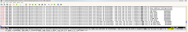
Figure 5 runsim.log
trans.log is generated from PCIe host VIP. trans.log records all transaction information coming in or going out of the VIP. Users can find traffic direction(DIR), TLP type, Tag, Address or BDF, 3 or 4 dword header of the TLP as shown in Figure 6
![]()
Figure 6 trans.log
The waveform generated is named as "inter.vpd". To open the waveform, go to simulation result directory and run
dve -full64 -vpd inter.vpd &
Questasim (TBD)
Running Questasim UVM tests will generate a ofs-agx7-pcie-attach/verification/sim_msim directory
• All build time logs are at ofs-agx7-pcie-attach/verification/sim_msim

• Each testcase will have separate directory inside sim ofs-agx7-pcie-attach/verification/sim_msim/<test_case_name>
There are two tracker or log files that are available: runsim.log and trans.log.
runsim.log is the simulation log file generated from Questasim. The test sequence prints useful information for debugging purpose, such as the base address for each function or block. For HE-LB and HE-MEM, key information such as SRC_ADDR, DST_ADDR, NUM_LINES, mode, req_len etc is printed out as shown in Figure 7
Figure 7 runsim.log
trans.log is generated from PCIe host VIP. trans.log records all transaction information coming in or going out of the VIP. Users can find traffic direction(DIR), TLP type, Tag, Address or BDF, 3 or 4 dword header of the TLP as shown in Figure 8
![]()
Figure 8 trans.log
The waveform generated is named as "vsim.wlf". To open the waveform, go to simulation result directory and run
vsim -view vsim.wlf &
6.9 UVM Coverage Analysis
For Intel® FPGA SmartNIC N6001-PL
The following command allows to run a single testcase with coverage enabled
gmake -f Makefile_VCS.mk cmplib_adp && gmake -f Makefile_VCS.mk build_adp DUMP=1 DEBUG=1 COV_FUNCTIONAL=1&& gmake -f Makefile_VCS.mk run TESTNAME=<TESTCASE-NAME> DUMP=1 DEBUG=1 COV_FUNCTIONAL=1 &
The following command shows how to merge and generate the coverage report
urg -dir <$VERDIR/sim/simv.vdb> <$VERDIR/sim/regression.vdb> -format both -dbname <regression_database_name>
This will generate both urgreport directory and
e.g "urg -dir <path1_till_simv.vdb> <path1_till_regression.vdb> <path2_till_regression.vdb> -report <dir> -format both -dbname <dirname>"
The following commands shows how to launch DVE and check the coverage reports
To open DVE of a single regression or testcase, execute:

    dve -full64 -cov -covdir simv.vdb regression.vdb &

To open DVE of a merged regression test, execute:

    dve -full64 -cov -covdir <dirname.vdb> &
Agilex® 7 FPGA F-Series Development Kit (2x F-Tile)
TBC
7 CSR Verification using UVM RAL
7.1 Overview
The UVM Register Layer provides a standard base class library that enable users to implement the object-oriented model to access the DUT registers and memories. The UVM Register Layer is also referred to as UVM Register Abstraction Layer (UVM RAL). Design registers can be accessed independently of the physical bus interface. i.e. by calling read/write methods. This is shown in Figure 9 below.
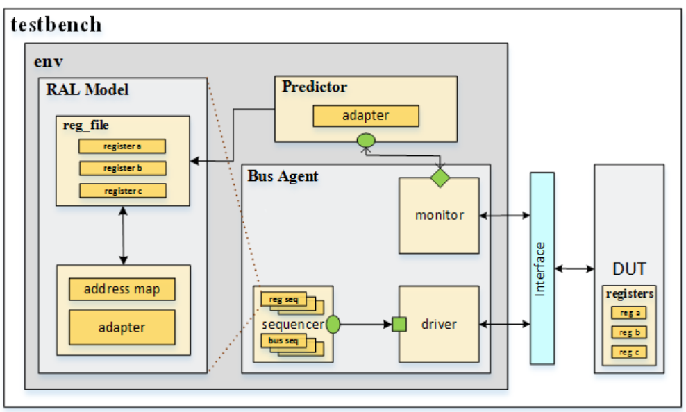
Figure 9 RAL UVM Testbench
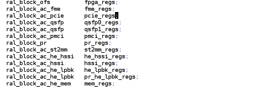
The RAL register models for different CSR's mimics the design registers. All RAL files are located here.
ofs-agx7-pcie-attach/verification/testbench/ral
The RAL model is generated through the Synopsys RALGEN tool and is used for CSR verification.
7.2 RAL Integration
For UVM RAL model integration to the environment, adapters for each CSR is implemented and integrated into the Testbench Environment. It is used to convert the PCIe bus sequence items into uvm_reg_bus_op and vice versa. The CSR test cases pick up all the registers from the respective CSR blocks and perform a default value, wr/rd check on them.
7.3 RAL Model Generation
Steps for RAL model generation
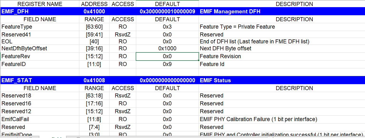
Excel(xls) file containing the registers is required. Make sure there are separate xls files for each CSR and the worksheet name must contain the name "reg_fields".
Excel sheet snapshot example below for EMIF_CSR.xls located at /ipss/mem/rtl/adp
• Navigate to ofs-agx7-pcie-attach/ofs-common/verification/common/scripts/ral
• Copy the excel file (xls) to the above area
• In the bash terminal run mk_ral.sh <Excel sheet name without extension > <output *.sv file name without ral_  prepended >
• The above steps generate two ral *.sv files. File with _cov suffix is a coverage enabled ral model.
• Copy *.sv files to ofs-agx7-pcie-attach/verification/testbench/ral

• As an example to generate ral_ac_ce.sv from AC_CE_CSR.xls file the command is

    mk_ral.sh AC_CE_CSR ac_ce
This generates two ral models (ral_ac_ce.sv and ral_ac_ce_cov.sv)
To add new registers
• To create new registers, copy existing ones and modify the cells in the xls. Make sure the last line is also a copied blank line
• Follow all the steps of RAL model generation
To Generate a RAL model when a new xls sheet is created for a new component
• Copy the relevant xls sheet to ofs-agx7-pcie-attach/ofs-common/verification/common/scripts/ral
• Follow all the steps of RAL model generation
7.4 Top Level Verification Architecture for CSR testing
7.4.1 Testbench components
The testbench components for RAL are defined below
• ral_reg_iofs_* (uvm_reg) generated by the steps as mentioned in section 5.3
The uvm register class is written by extending the uvm_reg. A register represents a set of fields that are accessible as a single entity Each register contains any number of fields, which mirror the values of the corresponding elements in hardware
• ral_block_iofs_* (uvm_block) generated in the same register file
A register model is an instance of a register block, which may contain any number of registers, register files, memories, and other blocks
• ral_block_ofs (uvm_block) – Contains all the CSR block instantiations
• Reg2vip_*_adapter (uvm_reg_adapter) – This class defines an interface for converting between uvm_reg_bus_op and a specific bus transaction. For each CSR a respective adapter is present
All the components are defined in ofs-agx7-pcie-attach/ofs-common/verification/testbench
Integration of components in testbench
• The RAL blocks and adapters for each CSR is instantiated in tb_env
• The bar range for each CSR is also set in the tb_env
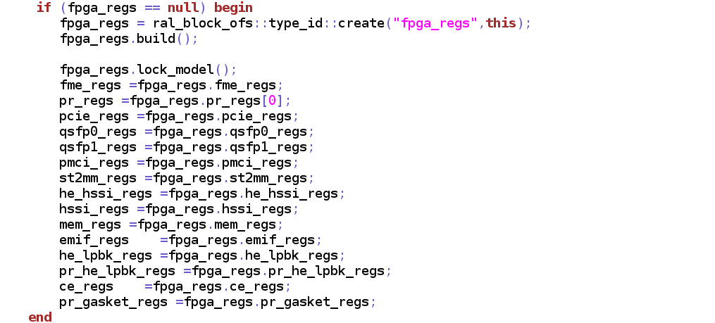
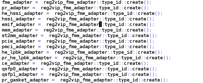
Sample Environment Integration snippets
8 Modifying UVM Testbench
The next sections describe what needs to be considered when modifying the UVM, adding a new interface to the testbench and creating a new UVM test for a customised OFS Accelerator platform.
8.1 Modifying UVM environment for new Shell Variant
OFS n6001 comprises a shell based on PCIe Gen4x16 and is named base_x16
This base_x16 shell is described by an RTL file list, IP File lists and setup scripts to complete the build flow
8.2 Modifying UVM environment and setting up Compile and Run flow
All the variants can mostly reuse the existing UVM infrastructure to setup the build and run flow
• Create directory under $OFS_BUILD_ROOT new variant e.g ofs-n9000
• Change directory to $OFS_BUILD_ROOT/ofs-n9000/verification/scripts
• modify Makefile it to point to the new RTL, IP and script files.
Following these three steps above will enable the build and sim flow to run the existing UVM TB and tests with new IOFS n9000 variant.
Adding a new interface requires signal connections in the testbench. An additional BFM or verification IP is needed to drive the new interface. The main testbench file tb_top.sv is found at the following location
ofs-agx7-pcie-attach/verification/testbench
8.3 Adding a new RAL directory
In case the design has many register changes and the user decides to generate all the new RAL models instead of reusing from existing base RAL models, the following steps will help to create and integrate a new RALDIR in the UVM environment.
• Generate the new RAL files in desired directory. Preferably under the "ofs-agx7-pcie-attach/verification/common/testbench"
• By default, the Makefile points to base FIM RAL so set the RALDIR path in the Makefile to the new generated RAL file directory
8.4 Modifying TB/Test files for new Variant
Create a define for the new variant. e.g 'define FIM_NEW. If you are modifying common files then add new logic under this define so other projects will not get affected with variant specific change.
If there are more changes, please create separate "testbench" and "test" folders under this new variant.
• Extend variant specific env file from base env file to add variant specific changes.
• Create new test/seq lib files in "tests" folder.
• Create new variant package, add new TB/Tests/Sequence lib files and also import the base package files.
If you are adding new files then make sure it's included in Makefile for the build+run flow.
8.5 UVM PCIe Drivers
The "svt_pcie_driver_app_transaction_base_sequence" is part of Synopsys PCIe VIP library. You can find the sequence definition in the following two directories
• Navigate to "$DESIGNWARE_HOME/vip/svt/pcie_svt/Q-2020.03/sverilog/src/vcs/svt_pcie_driver_app_transaction_sequence_collection.svp" file. All the base and PCIe sequences are defined in this file.

• When the OFS UVM build command is executed, it creates "vip" directory under "$OFS_BUILD_ROOT/ofs-agx7-pcie-attach/verification". You can also find the same sequence file at "$IOFS_BUILD_ROOT/ofs-agx7-pcie-attach/verification/vip/pcie_vip/src/sverilog/vcs/svt_pcie_driver_app_transaction_sequence_collection.sv"
Notices & Disclaimers
Intel® technologies may require enabled hardware, software or service activation. No product or component can be absolutely secure. Performance varies by use, configuration and other factors. Your costs and results may vary. You may not use or facilitate the use of this document in connection with any infringement or other legal analysis concerning Intel products described herein. You agree to grant Intel a non-exclusive, royalty-free license to any patent claim thereafter drafted which includes subject matter disclosed herein. No license (express or implied, by estoppel or otherwise) to any intellectual property rights is granted by this document, with the sole exception that you may publish an unmodified copy. You may create software implementations based on this document and in compliance with the foregoing that are intended to execute on the Intel product(s) referenced in this document. No rights are granted to create modifications or derivatives of this document. The products described may contain design defects or errors known as errata which may cause the product to deviate from published specifications. Current characterized errata are available on request. Intel disclaims all express and implied warranties, including without limitation, the implied warranties of merchantability, fitness for a particular purpose, and non-infringement, as well as any warranty arising from course of performance, course of dealing, or usage in trade. You are responsible for safety of the overall system, including compliance with applicable safety-related requirements or standards. © Intel Corporation. Intel, the Intel logo, and other Intel marks are trademarks of Intel Corporation or its subsidiaries. Other names and brands may be claimed as the property of others.
OpenCL and the OpenCL logo are trademarks of Apple Inc. used by permission of the Khronos Group™.