UVM Simulation User Guide: Open FPGA Stack for Intel Stratix® 10 FPGA
| Term | Description |
|---|---|
| AER | Advanced Error Reporting, The PCIe AER driver is the extended PCI Express error reporting capability providing more robust error reporting. |
| AFU | Accelerator Functional Unit, Hardware Accelerator implemented in FPGA logic which offloads a computational operation for an application from the CPU to improve performance. Note: An AFU region is the part of the design where an AFU may reside. This AFU may or may not be a partial reconfiguration region |
| BBB | Basic Building Block, Features within an AFU or part of an FPGA interface that can be reused across designs. These building blocks do not have stringent interface requirements like the FIM's AFU and host interface requires. All BBBs must have a (globally unique identifier) GUID. |
| BKC | Best Known Configuration, The exact hardware configuration Intel has optimized and validated the solution against. |
| BMC | Board Management Controller, Acts as the Root of Trust (RoT) on the Intel FPGA PAC platform. Supports features such as power sequence management and board monitoring through on-board sensors. |
| CSR | Command/status registers (CSR) and software interface, OFS uses a defined set of CSR's to expose the functionality of the FPGA to the host software. |
| DFL | Device Feature List, A concept inherited from OFS. The DFL drivers provide support for FPGA devices that are designed to support the Device Feature List. The DFL, which is implemented in RTL, consists of a self-describing data structure in PCI BAR space that allows the DFL driver to automatically load the drivers required for a given FPGA configuration. |
| FIM | FPGA Interface Manager, Provides platform management, functionality, clocks, resets and standard interfaces to host and AFUs. The FIM resides in the static region of the FPGA and contains the FPGA Management Engine (FME) and I/O ring. |
| FME | FPGA Management Engine, Provides a way to manage the platform and enable acceleration functions on the platform. |
| HEM | Host Exerciser Module, Host exercisers are used to exercise and characterize the various host-FPGA interactions, including Memory Mapped Input/Output (MMIO), data transfer from host to FPGA, PR, host to FPGA memory, etc. |
| Intel FPGA PAC D5005 | Intel FPGA Programmable Acceleration Card D5005, A high performance PCI Express (PCIe)-based FPGA acceleration card for data centers. This card is the target platform for the initial OFS release. |
| Intel VT-d | Intel Virtualization Technology for Directed I/O, Extension of the VT-x and VT-I processor virtualization technologies which adds new support for I/O device virtualization. |
| IOCTL | Input/Output Control, System calls used to manipulate underlying device parameters of special files. |
| JTAG | Joint Test Action Group, Refers to the IEEE 1149.1 JTAG standard; Another FPGA configuration methodology. |
| MMIO | Memory Mapped Input/Output, Users may map and access both control registers and system memory buffers with accelerators. |
| OFS | Open FPGA Stack, A modular collection of hardware platform components, open source software, and broad ecosystem support that provides a standard and scalable model for AFU and software developers to optimize and reuse their designs. |
| OPAE SDK | Open Programmable Acceleration Engine Software Development Kit, A collection of libraries and tools to facilitate the development of software applications and accelerators using OPAE. |
| PAC | Programmable Acceleration Card: FPGA based Accelerator card |
| PIM | Platform Interface Manager, An interface manager that comprises two components: a configurable platform specific interface for board developers and a collection of shims that AFU developers can use to handle clock crossing, response sorting, buffering and different protocols. |
| PR | Partial Reconfiguration, The ability to dynamically reconfigure a portion of an FPGA while the remaining FPGA design continues to function. In the context of Intel FPGA PAC, a PR bitstream refers to an Intel FPGA PAC AFU. Refer to Partial Reconfiguration support page. |
| RSU | Remote System Update, A Remote System Update operation sends an instruction to the Intel FPGA PAC D5005 device that triggers a power cycle of the card only, forcing reconfiguration. |
| SR-IOV | Single-Root Input-Output Virtualization, Allows the isolation of PCI Express resources for manageability and performance. |
| TB | Testbench, Testbench or Verification Environment is used to check the functional correctness of the Design Under Test (DUT) by generating and driving a predefined input sequence to a design, capturing the design output and comparing with-respect-to expected output. |
| UVM | Universal Verification Methodology, A modular, reusable, and scalable testbench structure via an API framework. |
| VFIO | Virtual Function Input/Output, An IOMMU/device agnostic framework for exposing direct device access to userspace. |
1 Overview
1.1 About this Document
This document serves as a set-up and user guide for the UVM simulation tool using OFS. After reviewing the document, you will be able to:
- Set-up the UVM verification tool suite
- Run pre-existing UVM unit tests and also create new UVM tests for your design
2 Introduction to UVM
OFS (Open FPGA Stack) provides a UVM (Universal Verification Methodology) environment for the FIM (FPGA Interface Manager) with a modular, reusable, and scalable testbench structure via an API framework.
The framework consists of a FIM Testbench which is UVM compliant and integrates third party VIPs from Synopsys for PCI Express, Arm® AMBA® 4 AXI4-Streaming interface and Arm® AMBA® 4 AXI4-Memory Mapped interface for comprehensive verification. The user will need to acquire licenses for these VIPs to use this Testbench. UVM RAL (Register Abstaction Layer) is used for CSR (Command and Status Registers) verification.
The qualified verification IPs will help to detect incorrect protocol behavior, help to focus on FIM features and accelerate the verification process.
Verification components include:
- FIM monitor to detect correct design behavior
- FIM assertions for signal level integrity testing
- Arm AMBA Arm® AMBA® 4 AXI4 scoreboards to check data integrity
- FIM coverage to collect functional data
3 Testbench Architecture
The testbench connects to the full chip that includes major RTL blocks depicted in Figure 1.
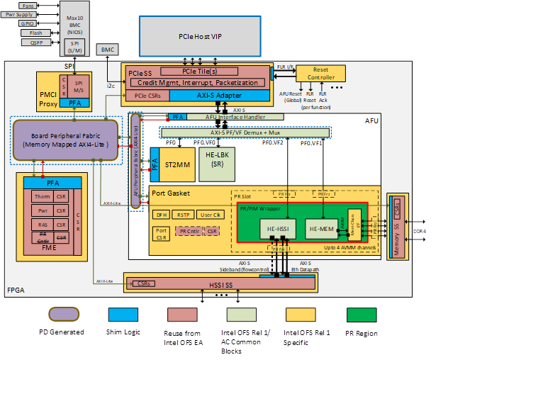
Figure 1 Testbench Diagram
The major interface is between the Xeon and FPGA where PCIe Verification IP is connected to PCIe Subsystem. Therefore, as a full chip simulation environment, PCIe host VIP is the sole VIP/BFM used. PCIe host VIP connects to PCIe device which resides in FPGA in serial mode.
4 Testbench Infrastructure
4.1 Traffic Flow
PCIe Host, as the master of FPGA, initiates MMIO read/write requests to FPGA to program registers. The PCIe host also passively receives memory requests from FPGA to read from or write to host memory.
4.2 Link Up and Enumeration
With serial mode connection between PCIe host and device, link training and enumeration has to be done before the regular traffic starts.
4.2.1 Link Up
Linkup sequence(pcie_device_bring_up_link_sequence) is part of configure sequence(ofs_config_seq), which is started in UVM configure phase.
4.2.2 Enumeration
PCIe host driver needs to retrieve information from the device hard IP and program necessary configuration space registers, such as PF/VF BAR values. This is done in enumerate_seq, which follows link up sequence in configure sequence(ofs_config_seq).
4.2.3 PF/VF BAR
PF0 BAR0 is set in the base sequence and can be randomized. During enumeration, PF0 BAR0, along with PCIe device hard IP configuration, derives other PF and VF BAR values. These BAR values are stored into base sequence variables and can be used throughout any test sequences that extend the base sequence.
4.3 MMIO APIs
The base sequence provides APIs for 32-bit and 64-bit MMIO read/write accesses, as well as blocking or non-blocking for MMIO read as described in Table 1. The users can use MMIO APIs without knowing the underlining PCIe sequence items.
| Name | API |
|---|---|
| 32-bit MMIO Write | task mmio_write32(input bit [63:0] addr_, input bit [31:0] data_); |
| 64-bit MMIO Write | task mmio_write64(input bit [63:0] addr_, input bit [63:0] data_); |
| 32-bit MMIO Read | task mmio_read32(input bit [63:0] addr_, output bit [31:0] data_, input blocking_ = 1); |
| 64-bit MMIO Read | task mmio_read64(input bit [63:0] addr_, output bit [63:0] data_, input blocking_ = 1); |
Table 1 MMIO APIs
4.4 RAL
UVM RAL is integrated in the testbench providing alternative ways of accessing CSRs in test sequences. RAL is generated from an excel format CSR specification where register name, field, offset, bitmap, attribute, and description are specified.
4.5 VIP DUT Connection
PCIe host verification IP and DUT connection is achieved by connecting 16 bits lanes. The module for connection from VIP is svt_pcie_device_agent_serdes_x16_x8g_hdl.
5 Test Plan
The test plan consists of four major categories: MMIO path, HE-LB, HE-MEM, HE-HSSI and interrupt tests.
5.1 MMIO Path
The tests under this category exercise MMIO path including all destination functions or blocks as well as PF/VF mux and different fabrics.
5.2 HE-LB
The tests under this category target HE-LB function only. Software which test sequences needs to configure HE-LB CSRs before starting it. These CSRs include SRC_ADDR, DST_ADDR, DSM_ADDR, NUM_LINES, CFG etc.
If HE-LB is configured to have memory read transactions, PCIe host memory has to be initialized before HE-LB is started. This is done by svt_pcie_mem_target_service sequence. In other words, PCIe host VIP programs its internal memory model entries in backdoor way. The same process applies to DSM memory entry.
Once HE-LB is started, HE-LB will function based on what it is programmed to do. When HE-LB is done with all necessary memory transactions, it will perform a final memory write to DSM memory entry. Since the software does not know when hardware is done, software polls DSM memory entry periodically until the DSM status bit is asserted.
For loopback mode, data is compared between source buffer and destination buffer in host memory.
RTL statistic counters are also compared against the corresponding variables inside the test sequence at the end of the simulation.
5.3 HE-MEM
HE-MEM tests are duplicates from HE-LB with MMIO to CSRs targeting HE-MEM instead of HE-LB.
The DDR simulation model is inside memory controller IP when being generated.
5.4 HE-HSSI
HE-HSSI has indirect registers that are associated with HSSI subsystem, MMIO for indirect registers is different from other functions.
5.4.1 Indirect Registers
To obtain access to indirect registers, either reading or writing, a MMIO write must be performed.
5.4.2 TX Loopback
In TX loopback, HE-HSSI initiates ethernet packets to HSSI subsystem and the packets are looped back to HE-HSSI. The loopback is achieved by hard-wiring HSSI TX and RX lanes. This is done inside RTL and for simulation purposes only.
5.5 Interrupt Test
The test plan covers the basic interrupt flow for FME error, PORT error and user AFU interrupts. The MSI-X table must be programmed in PF0 BAR4. Corresponding PBA bit is expected to be asserted.
5.6 Performance Test
Performance tests are derived from HE-LB tests and they are directed tests. At the end of the simulation, performance number is calculated and printed to terminal and a log file.
5.7 CSR Test
CSR consists of two parts.
5.7.1 Reset Value Check
Front-door MMIO read data is compared against RAL register reset value out of reset.
5.7.2 RW Attribute CSR
MMIO write-read-compare is performed after reset value check for RW attribute CSRs.
6 Checking Mechanism
Since there is only PCIe host verification component in testbench, data checking is done by a self-checking mechanism in the test sequence.
6.1 Protocol Violation
PCIe host VIP has built-in protocol checking on TLP received from FPGA. Abnormal responses are also flagged by the VIP.
Internal AXI Streaming interface has integrated RTL assertion to check AXI Streaming protocol violations.
6.2 Data Checking
Data checking is done by self-checking inside a test sequence. MMIO write/read/compare to read-writable CSRs is done inside a sequence.
For memory transactions initiated by functions, backdoor reads from host memory on source buffer and destination buffer is done inside a sequence. Data is compared in case of loopback mode.
6.3 Counter Checking
RTL statistic counters records the number of transactional information that can be read at the end of the simulation and compared against the test expected number.
6.4 AFU Error CSR
AFU interface handler provides an error log for illegal transactions that can be read at the end of the simulation.
7 UVM set-up
To run the tutorial steps in this guide requires the following development environment:
| Item | Version |
|---|---|
| Intel Quartus Prime Pro | Intel Quartus Prime Pro 23.4 |
| Simulator (VCS) | Synopsys VCS S-2021.09-SP1 or newer for UVM simulation of top level FIM |
| Simulator (Questasim) | Questasim 2023.4 or newer for UVM simulation of top level FIM |
7.1 UVM Prerequisite
Retrieve OFS repositories.
The OFS FIM source code is included in the GitHub repository. Create a new directory to use as a clean starting point to store the retrieved files. The following is a short description of each repository, followed by the git commands for cloning. The instructions section uses the HTTPS git method for cloning repositories. Cloning the repo using the HTTPS method requires a personal access token. Please see this blog post for information about obtaining a personal access token Token authentication requirements for Git operations.
Navigate to the location for storage of OFS source, create the top-level source directory and clone OFS repositories.
$ mkdir ofs-2024.1-1
$ cd ofs-2024.1-1
$ export OFS_BUILD_ROOT=$PWD
$ git clone --recurse-submodules https://github.com/OFS/ofs-d5005

Cloning into 'ofs-d5005' ...
Username for 'https://github.com': <<Enter your git hub username>>
Password for 'https://<<Your username>>': <<Enter your personal access token>>
remote: Enumerating objects:  ....
...
...
Resolving deltas  ..., done.

$ cd ofs-d5005
$ git checkout tags/ofs-2024.1-1
Verify that the correct tag/branch have been checked out
7.2 License Requirements
The FIM Testbench is UVM compliant and integrates third party VIPs from Synopsys for PCI Express, Arm® AMBA® 4 AXI4-Streaming interface and Arm® AMBA® 4 AXI4-Memory Mapped interface for comprehensive verification. The user will need to acquire licenses for these VIPs to use this TB. UVM RAL (Register Abstraction Layer) is used for CSR Verification.
The Qualified Verification IPs will help to detect incorrect protocol behavior easily, help to focus on BBS features and accelerate the verification process.
- VCS & DVE
- SNPS-Assertions
- Verdi
- VerdiCoverage
- VerdiSimDB
- VerdiTransactionDebugUltra
- VIP-AMBA-AXI-SVT
- VIP-AMBA-STREAM-SVT
- VIP-PCIE-SVT
- VIP-PCIE-TS-SVT
- VIP-PCIE-G3-OPT-SVT
7.3 Software Tools Requirements
The following tools are required for successful UVM set-up
- Python 3.6.8
- Synopsys PCIE and AMBA AXI UVM VIP Q-2020.03A License
- Synopsys Verdi R-2020.12-SP2 License
Note: Makefile can be modified to use DVE instead of Verdi
- VCS R-2020.12-SP2 License
7.4 Creating a Software Tools Script
The UVM tool set-up is best done by creating a simple set-up script so all applicable tools are sourced before running the tests.
The following environment variables can be pasted into a script and used prior to running the UVM verification environment
License Files
The license environment variables LM_LICENSE_FILE and SNPSLMD_LICENSE_FILE can point to a server license on your system.
General Environment Variables
Quartus Tools
export QUARTUS_HOME=<user_path>/intelFPGA_pro/23.4/quartus
export QUARTUS_ROOTDIR=$QUARTUS_HOME
export QUARTUS_INSTALL_DIR=$QUARTUS_ROOTDIR
export QUARTUS_ROOTDIR_OVERRIDE=$QUARTUS_ROOTDIR
export IMPORT_IP_ROOTDIR=$QUARTUS_ROOTDIR/../ip
export QSYS_ROOTDIR=$QUARTUS_ROOTDIR/../qsys/bin
export PATH=$QUARTUS_HOME/bin:$QUARTUS_HOME/qsys/bin:$QUARTUS_HOME/sopc_builder/bin/:$PATH
Synopsys Verification Tools
export DESIGNWARE_HOME=<user_path>/synopsys/vip_common/vip_Q-2020.03A
export PATH=$DESIGNWARE_HOME/bin:$PATH
export UVM_HOME=<user_path>/synopsys/vcsmx/S-2021.09-SP1/linux64/rhel/etc/uvm
export VCS_HOME=<user_path>/synopsys/vcsmx/S-2021.09-SP1/linux64/rhel
export PATH=$VCS_HOME/bin:$PATH
export VERDIR=$OFS_ROOTDIR/verification
export VIPDIR=$VERDIR
QuestaSIM Verification Tools
export MTI_HOME=<user_path>/mentor/questasim/2023.4/linux64
export PATH=$MTI_HOME/linux_x86_64/:$MTI_HOME/bin/:$PATH
export QUESTA_HOME=$MTI_HOME
8 Running a UVM Simulation Test and Analysing Results
8.1 Simulation
The default simulator used in this document is Synopsys VCS-MX but there will be references to Questasim. Users can refer to the options and adopt the options for other simulators.
The script is a makefile that calls vlogan, vcs and simv for compilation, elaboration and simulation, respectively
8.2 File Structure
After cloning the repo, the verification and ofs-common directories contain all UVM verification related files. The directory structure is shown in Figure 2 below.
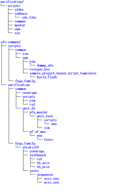
Figure 2 UVM Verification Directory File Structure
ofs-d5005/testbench has a testbench, uvm env, virtual sequencer, RAL etc.
ofs-d5005/verification/tests contains all uvm tests and sequences.
Users can run the simulation under "ofs-d5005/verification/scripts" directory and the simulation result is outputted to a "sim" directory for Synopsys VCS or "sim_msim" for Questasim.
The simulation result folder is named after the test name with increasing suffix number. If user runs the same test multiple times, the suffix is incremented by 1 each time.
8.3 UVM Test Suite
The UVM environment contains a variety of tests that have been developed to test out the FIM portion of OFS.
The table below lists out the "Test Name" which will be used on the command line to execute the test, the "Test Scenario" and the "Checking Criteria".
Tests are located at ofs-d5005/verification/tests
| Test Name | DUT Scope | Test Scenario | Checking Criteria |
|---|---|---|---|
| dfh_walking_test | DFH | DHF walking | offset checking, eol checking |
| flr_reset_test | FLR Reset | FLR reset to all PFs | Reset checking |
| flr_vf0_reset_test | FLR Reset | FLR reset to VF0 | Reset checking |
| flr_vf1_reset_test | FLR Reset | FLR reset to VF1 | Reset checking |
| flr_vf2_reset_test | FLR Reset | FLR reset to VF2 | Reset checking |
| fme_csr_test | FME CSR | CSR accesses | data checking |
| fme_hemem_intr_test | Interrupt | FME and HE MEM interrupt | Interrupts assertion, PBA bits check |
| fme_intr_test | Interrupt | FME error interrupt | Interrupts assertion, PBA bits check |
| he_hssi_csr_test | HE-HSSI | CSR accesses for HSSI | data checking |
| he_hssi_err_test | HE-HSSI | Error Cases | counter checking |
| he_hssi_rx_lpbk_test | HE-HSSI | RX loopback | data checking |
| he_hssi_tx_lpbk_test | HE-HSSI | TX loopback | counter checking |
| he_lpbk_cont_test | HE-LPBK | Continuous mode/LPBK mode, random num_lines, addresses, req_len | data checking |
| he_lpbk_long_rst_test | HE-MEM | Multiple iterations of he_lpb_seq with soft reset HE-LB in middle | data checking, counter checking |
| he_lpbk_long_test | HE-MEM | Multiple iterations of he_lpb_seq with STOP HE-LB in middle | data checking, counter checking |
| he_lpbk_port_rst_test | HE-LPBK | Loopback mode. Randomize num_lines, addresses, req_len with port rst | data checking |
| he_lpbk_rd_cont_test | HE-LPBK | Read only mode/ Continuous mode. Randomize num_lines, addresses, req_len | data checking, counter checking |
| he_lpbk_rd_test | HE-LPBK | Read only mode. Randomize num_lines, addresses, req_len | counter checking |
| he_lpbk_reqlen1_test | HE-LPBK | Loopback mode. 128 CLs, req_len = 1CL, random addresses | data checking, counter checking |
| he_lpbk_reqlen2_test | HE-LPBK | Loopback mode. 128 CLs, req_len = 2CL, random addresses. | data checking, counter checking |
| he_lpbk_reqlen4_test | HE-LPBK | Loopback mode. 128 CLs, req_len = 4CL, random addresses | data checking, counter checking |
| he_lpbk_reqlen8_test | HE-LPBK | Loopback mode. 128 CLs, req_len = 8CL, random addresses | data checking, counter checking |
| he_lpbk_test | HE-LPBK | Loopback mode. Randomize num_lines, addresses, req_len | data checking, counter checking |
| he_lpbk_thruput_contmode_test | HE-LPBK | Continuous mode, Read/Write mode. 50/50. Randomize num_lines, addresses req_len | data checking, counter checking |
| he_lpbk_thruput_test | HE-LPBK | Read/Write mode. 50/50. Randomize num_lines, addresses, req_len | counter checking |
| he_lpbk_wr_cont_test | HE-LPBK | Write only mode/ Continuous mode. Randomize num_lines, addresses, req_len | data checking, counter checking |
| he_lpbk_wr_test | HE-LPBK | Write only mode. Randomize num_lines, addresses, req_len | counter checking |
| he_mem_cont_test | HE-MEM | Continuous mode/LPBK mode, random num_lines, addresses, req_len | data checking |
| he_mem_lpbk_long_rst_test | HE-LPBK | Multiple iterations of he_lpb_seq with soft reset HE-LB in middle | data checking, counter checking |
| he_mem_lpbk_long_test | HE-LPBK | Multiple iterations of he_lpb_seq with STOP HE-LB in middle | data checking, counter checking |
| he_mem_lpbk_reqlen1_test | HE-MEM | Loopback mode. 128 CLs, req_len = 1CL, random addresses. | data checking, counter checking |
| he_mem_lpbk_reqlen2_test | HE-MEM | Loopback mode. 128 CLs, req_len = 2CL, random addresses. | data checking, counter checking |
| he_mem_lpbk_reqlen4_test | HE-MEM | Loopback mode. 128 CLs, req_len = 4CL, random addresses | data checking, counter checking |
| he_mem_lpbk_test | HE-MEM | Loopback mode. Randomize num_lines, addresses, req_len | data checking, counter checking |
| he_mem_rd_cont_test | HE-MEM | Read only mode/ Continuous mode. Randomize num_lines, addresses, req_len | data checking, counter checking |
| he_mem_rd_test | HE-MEM | Read only mode. Randomize num_lines, addresses, req_len | counter checking |
| he_mem_thruput_contmode_test | HE-MEM | Continuous mode, Read/Write mode. 50/50. Randomize num_lines, addresses, req_len | data checking, counter checking |
| he_mem_thruput_test | HE-MEM | Read/Write mode. 50/50. Randomize num_lines, addresses, req_len | counter checking |
| he_mem_wr_cont_test | HE-MEM | Write only mode/ Continuous mode. Randomize num_lines, addresses, req_len | data checking, counter checking |
| he_mem_wr_test | HE-MEM | Write only mode. Randomize num_lines, addresses, req_len | counter checking |
| he_random_long_test | All HE's | Enable all HEs and randomize modes for multiple iterations | data checking if in lpbk mode, counter checking |
| he_random_test | All HEs | Enable all HEs and randomize modes | data checking if in lpbk mode, counter checking |
| hehssi_csr_test | HE-HSSI | CSR accesses for Traffic Control Mail box registers | data checking |
| helb_csr_test | HE-LPBK | CSR accesses | data checking |
| helb_rd_1cl_test | Performance | HE-LB; ReqLen = 1CL; 1024 CLs; Read only mode | data checking, counter checking |
| helb_rd_2cl_test | Performance | HE-LB; ReqLen = 2CL; 1024 CLs; Read only mode | data checking, counter checking |
| helb_rd_4cl_test | Performance | HE-LB; ReqLen = 4CL; 1024 CLs; Read only mode | data checking, counter checking |
| helb_thruput_1cl_test | Performance | HE-LB; ReqLen = 1CL; 1024 CLs; Thruput mode | data checking, counter checking |
| helb_thruput_2cl_test | Performance | HE-LB; ReqLen = 2CL; 1024 CLs; Thruput mode | data checking, counter checking |
| helb_thruput_4cl_test | Performance | HE-LB; ReqLen = 4CL; 1024 CLs; Thruput mode | data checking, counter checking |
| helb_wr_1cl_test | Performance | HE-LB; ReqLen = 1CL; 1024 CLs; Write only mode | data checking, counter checking |
| helb_wr_2cl_test | Performance | HE-LB; ReqLen = 2CL; 1024 CLs; Write only mode | data checking, counter checking |
| helb_wr_4cl_test | Performance | HE-LB; ReqLen = 4CL; 1024 CLs; Write only mode | data checking, counter checking |
| hemem_csr_test | HE-MEM | CSR accesses | data checking |
| hemem_intr_test | Interrupt | HE MEMN Interrupt | Interrupts assertion, PBA bits check |
| malformedtlp_test | Protocol Checker | Checks for different PCIe Protocol error generation (upstram/downstream) and check the clear mechanism of AFU for these detected protocol errors. 1. Apply the error 2. Wait 5us 1us 3. Set the port reset bit true and then false again (within 1us) (You will not be able to perform a read-modify-write because F's will be returned on reads. Write a 0x5 to set and a 0x4 to clear) 4. Wait 124us 135us (or 7.5us 28us if MMIO_TIMEOUT_CYCLES is 512.) 5. Read bit 31 of the AFU_INTF_ERROR, BlockingTraffic. If it is set it means that we did not wait long enough in step 4 6. Read the AFU_INTF_ERROR register, Be sure only the expected error(s) are set 7. Read the AFU_INTF_FIRST_ERROR CSR. Be sure only one error bit is set and it is the expected one 8. Clear the errors in the AFU_INTF_ERROR CSR by writing one to the bits that are set 9. Read the AFU_INTF_FIRST_ERROR CSR. Be sure all bits are cleared | Check AFU_INTF_ERROR and AFU_INTF_FIRST_ERROR register is getting set with correct error vector. After clearing the error register,check if normal transcation are completing. |
| maxpayloaderror_test | Protocol Checker | Checks for different PCIe Protocol error generation (upstram/downstream) and check the clear mechanism of AFU for these detected protocol errors. 1. Apply the error 2. Wait 5us 1us 3. Set the port reset bit true and then false again (within 1us) (You will not be able to perform a read-modify-write because F's will be returned on reads. Write a 0x5 to set and a 0x4 to clear) 4. Wait 124us 135us (or 7.5us 28us if MMIO_TIMEOUT_CYCLES is 512.) 5. Read bit 31 of the AFU_INTF_ERROR, BlockingTraffic. If it is set it means that we did not wait long enough in step 4 6. Read the AFU_INTF_ERROR register, Be sure only the expected error(s) are set 7. Read the AFU_INTF_FIRST_ERROR CSR. Be sure only one error bit is set and it is the expected one 8. Clear the errors in the AFU_INTF_ERROR CSR by writing one to the bits that are set 9. Read the AFU_INTF_FIRST_ERROR CSR. Be sure all bits are cleared | Check AFU_INTF_ERROR and AFU_INTF_FIRST_ERROR register is getting set with correct error vector. After clearing the error register,check if normal transcation are completing. |
| MaxTagError_test | Protocol Checker | Checks for different PCIe Protocol error generation (upstram/downstream) and check the clear mechanism of AFU for these detected protocol errors. 1. Apply the error 2. Wait 5us 1us 3.Set the port reset bit true and then false again (within 1us) (You will not be able to perform a read-modify-write because F's will be returned on reads. Write a 0x5 to set and a 0x4 to clear) 4. Wait 124us 135us (or 7.5us 28us if MMIO_TIMEOUT_CYCLES is 512.) 5. Read bit 31 of the AFU_INTF_ERROR, BlockingTraffic. If it is set it means that we did not wait long enough in step 4 6. Read the AFU_INTF_ERROR register, Be sure only the expected error(s) are set 7. Read the AFU_INTF_FIRST_ERROR CSR. Be sure only one error bit is set and it is the expected one 8. Clear the errors in the AFU_INTF_ERROR CSR by writing one to the bits that are set 9. Read the AFU_INTF_FIRST_ERROR CSR. Be sure all bits are cleared | Check AFU_INTF_ERROR and AFU_INTF_FIRST_ERROR register is getting set with correct error vector. After clearing the error register,check if normal transcation are completing. |
| mini_smoke_test | All HEs | shorter simpler version of random test for turn-in sanity check | data checking if in lpbk mode, counter checking |
| mmio_64b_bar_test | PCIe MMIO Path | 64-bit bar addess for MMIO | data checking |
| mmio_stress_nonblocking_test | PF/VF Mux/Demux | Stressing MMIO on PF/VF Mux/Demux with non-blocking MMIO reads | data checking |
| mmio_stress_test | PF/VF Mux/Demux | Stressing MMIO on PF/VF Mux/Demux | data checking |
| mmio_test | PCIe MMIO Path | MMIO targeting PF0(ST2MM, FME, PMCI, HSSI SS), PF1, PF1.VF1, PF1.VF2 | data checking |
| mmio_unimp_test | PCIe MMIO Path | MMIO acccess to unimplemented addresses | MMIO checking |
| MMIODataPayloadOverrun_test | Protocol Checker | Checks for different PCIe Protocol error generation (upstram/downstream) and check the clear mechanism of AFU for these detected protocol errors. 1. Apply the error 2. Wait 5us 1us 3. Set the port reset bit true and then false again (within 1us) (You will not be able to perform a read-modify-write because F's will be returned on reads. Write a 0x5 to set and a 0x4 to clear) 4. Wait 124us 135us (or 7.5us 28us if MMIO_TIMEOUT_CYCLES is 512.) 5. Read bit 31 of the AFU_INTF_ERROR, BlockingTraffic. If it is set it means that we did not wait long enough in step 4 6. Read the AFU_INTF_ERROR register, Be sure only the expected error(s) are set 7. Read the AFU_INTF_FIRST_ERROR CSR. Be sure only one error bit is set and it is the expected one 8. Clear the errors in the AFU_INTF_ERROR CSR by writing one to the bits that are set 9. Read the AFU_INTF_FIRST_ERROR CSR. Be sure all bits are cleared | Check AFU_INTF_ERROR and AFU_INTF_FIRST_ERROR register is getting set with correct error vector. After clearing the error register,check if normal transcation are completing. |
| MMIOInsufficientData_test | Protocol Checker | Checks for different PCIe Protocol error generation (upstram/downstream) and check the clear mechanism of AFU for these detected protocol errors. 1. Apply the error 2. Wait 5us 1us 3. Set the port reset bit true and then false again (within 1us) (You will not be able to perform a read-modify-write because F's will be returned on reads. Write a 0x5 to set and a 0x4 to clear) 4. Wait 124us 135us (or 7.5us 28us if MMIO_TIMEOUT_CYCLES is 512.) 5. Read bit 31 of the AFU_INTF_ERROR, BlockingTraffic. If it is set it means that we did not wait long enough in step 4 6. Read the AFU_INTF_ERROR register, Be sure only the expected error(s) are set 7. Read the AFU_INTF_FIRST_ERROR CSR. Be sure only one error bit is set and it is the expected one 8. Clear the errors in the AFU_INTF_ERROR CSR by writing one to the bits that are set 9. Read the AFU_INTF_FIRST_ERROR CSR. Be sure all bits are cleared | Check AFU_INTF_ERROR and AFU_INTF_FIRST_ERROR register is getting set with correct error vector. After clearing the error register,check if normal transcation are completing. |
| MMIOTimedout_test | Protocol Checker | Checks for different PCIe Protocol error generation (upstram/downstream) and check the clear mechanism of AFU for these detected protocol errors. 1. Apply the error 2. Wait 5us 1us 3. Set the port reset bit true and then false again (within 1us) (You will not be able to perform a read-modify-write because F's will be returned on reads. Write a 0x5 to set and a 0x4 to clear) 4. Wait 124us 135us (or 7.5us 28us if MMIO_TIMEOUT_CYCLES is 512.) 5. Read bit 31 of the AFU_INTF_ERROR, BlockingTraffic. If it is set it means that we did not wait long enough in step 4 6. Read the AFU_INTF_ERROR register, Be sure only the expected error(s) are set 7. Read the AFU_INTF_FIRST_ERROR CSR. Be sure only one error bit is set and it is the expected one 8. Clear the errors in the AFU_INTF_ERROR CSR by writing one to the bits that are set9. Read the AFU_INTF_FIRST_ERROR CSR. Be sure all bits are cleared 9. Read the AFU_INTF_FIRST_ERROR CSR. Be sure all bits are cleared | Check AFU_INTF_ERROR and AFU_INTF_FIRST_ERROR register is getting set with correct error vector. After clearing the error register,check if normal transcation are completing. |
| msix_csr_test | MSIX CSR | CSR accesses | data checking |
| pmci_csr_test | PMCI CSR | CSR accesses | data checking |
| port_gasket_csr_test | PORT GASKET | Port Gasket CSR test | port csr checking |
| TxMWrDataPayloadOverrun_test | Protocol Checker | Checks for different PCIe Protocol error generation (upstram/downstream) and check the clear mechanism of AFU for these detected protocol errors. 1. Apply the error 2. Wait 5us 1us 3. Set the port reset bit true and then false again (within 1us) (You will not be able to perform a read-modify-write because F's will be returned on reads. Write a 0x5 to set and a 0x4 to clear) 4. Wait 124us 135us (or 7.5us 28us if MMIO_TIMEOUT_CYCLES is 512.) 5. Read bit 31 of the AFU_INTF_ERROR, BlockingTraffic. If it is set it means that we did not wait long enough in step 4 6. Read the AFU_INTF_ERROR register, Be sure only the expected error(s) are set 7. Read the AFU_INTF_FIRST_ERROR CSR. Be sure only one error bit is set and it is the expected one 8. Clear the errors in the AFU_INTF_ERROR CSR by writing one to the bits that are set 9. Read the AFU_INTF_FIRST_ERROR CSR. Be sure all bits are cleared | Check AFU_INTF_ERROR and AFU_INTF_FIRST_ERROR register is getting set with correct error vector. After clearing the error register,check if normal transcation are completing |
| TxMWrInsufficientData_test | Protocol Checker | Checks for different PCIe Protocol error generation (upstram/downstream) and check the clear mechanism of AFU for these detected protocol errors. 1. Apply the error 2. Wait 5us 1us 3. Set the port reset bit true and then false again (within 1us) (You will not be able to perform a read-modify-write because F's will be returned on reads. Write a 0x5 to set and a 0x4 to clear) 4. Wait 124us 135us (or 7.5us 28us if MMIO_TIMEOUT_CYCLES is 512.) 5. Read bit 31 of the AFU_INTF_ERROR, BlockingTraffic. If it is set it means that we did not wait long enough in step 4 6. Read the AFU_INTF_ERROR register, Be sure only the expected error(s) are set 7. Read the AFU_INTF_FIRST_ERROR CSR. Be sure only one error bit is set and it is the expected one 8. Clear the errors in the AFU_INTF_ERROR CSR by writing one to the bits that are set 9. Read the AFU_INTF_FIRST_ERROR CSR. Be sure all bits are cleared | Check AFU_INTF_ERROR and AFU_INTF_FIRST_ERROR register is getting set with correct error vector. After clearing the error register,check if normal transcation are completing |
| UnexpMMIORspErr_test | Protocol Checker | Checks for different PCIe Protocol error generation (upstram/downstream) and check the clear mechanism of AFU for these detected protocol errors. 1. Apply the error 2. Wait 5us 1us 3. Set the port reset bit true and then false again (within 1us) (You will not be able to perform a read-modify-write because F's will be retuened on resds. Write a 0x5 to set and a 0x4 to clear) 4. Wait 124us 135us (or 7.5us 28us if MMIO_TIMEOUT_CYCLES is 512.) 5. Read bit 31 of the AFU_INTF_ERROR, BlockingTraffic. If it is set it means that we did not wait long enough in step 4 6. Read the AFU_INTF_ERROR register, Be sure only the expected error(s) are set 7. Read the AFU_INTF_FIRST_ERROR CSR. Be sure only one error bit is set and it is the expected one 8. Clear the errors in the AFU_INTF_ERROR CSR by writing one to the bits that are set 9. Read the AFU_INTF_FIRST_ERROR CSR. Be sure all bits are cleared | Check AFU_INTF_ERROR and AFU_INTF_FIRST_ERROR register is getting set with correct error vector. After clearing the error register,check if normal transcation are completing |
The next section describes how to compile and build the UVM environment prior to running each UVM test and analyzing the results in the log files
8.4 IP Compile
Synopsys VCS
To compile all IPs for the Synopsys VCS simulater:
Questasim
To compile all IPs for the Questasim simulater:
8.5 RTL & Test Bench Compile
The RTL file list for compilation is located here: verification/scripts/rtl_comb.f
The TB file list for compilation is located here: verification/scripts/ver_list.f
Synopsys VCS
To compile RTL and Testbench for the Synopsys VCS simulater
Questasim
To compile RTL and Testbench for the Questasim simulater
8.6 IP and RTL & Test Bench Compile
Synopsys VCS
If the user wants to compile all IPs and RTL Testbench in one command for Synopsys VCS then follow the procedure below
Questasim
If the user wants to compile all IPs and RTL Testbench in one command for Questasim then follow the procedure below
Synopsys VCS
To run a simulation for Synopsys VCS:
Questasim
To run a simulation for Questasim:
Synopsys VCS
To dump the waveform, "DUMP=1" must be added into the command line for Synopsys VCS build and simulation.
    ofs-d5005/verification/scripts  gmake -f Makefile_VCS.mk build DUMP=1

    ofs-d5005/verification/scripts  gmake -f Makefile_VCS.mk run TESTNAME=<test_case_name> DUMP=1
Questasim
To dump the waveform, "DUMP=1" must be added into the command line for Questasim build and simulation.
    ofs-d5005/verification/scripts  gmake -f Makefile_MSIM.mk build DUMP=1

    ofs-d5005/verification/scripts  gmake -f Makefile_MSIM.mk run TESTNAME=<test_case_name> DUMP=1
There are some optimizations in the Table below for convenience if you want to bypass some commands for both Synopsys VCS and Questasim:
| Command (Synopsys VCS) | Command (Questasim) | Details |
|---|---|---|
| gmake -f Makefile_VCS.mk build_all DUMP=1 | gmake -f Makefile_MSIM.mk build_all DUMP=1 | compile IP + compile RTL |
| gmake -f Makefile_VCS.mk build_run TESTNAME= DUMP=1 | gmake -f Makefile_MSIM.mk build_run TESTNAME= DUMP=1 | compile RTL + run test |
| gmake -f Makefile_VCS.mk do_it_all TESTNAME= DUMP=1 | gmake -f Makefile_MSIM.mk do_it_all TESTNAME= DUMP=1 | compile IP, RTL and run test |
| gmake -f Makefile_VCS.mk rundb TESTNAME= DUMP=1 | gmake -f Makefile_MSIM.mk rundb TESTNAME= DUMP=1 | run test in sim dir + over-writes content |
8.7 UVM Regression Test
cd $VERDIR/scripts

For Regression in VCS with top/test package, execute the following command
    python uvm_regress.py -l -n 8 -s vcs -c

Results are created in a sim directory ($VERDIR/sim) with individual testcase log dir

For Regression in MSIM with top/test package, execute the following command
    python uvm_regress.py -l -n 8 -s msim -c
Results are created in a sim directory ($VERDIR/sim_msim) with individual testcase log dir
8.8 UVM Waveform and Transcript Analysis
Synopsys VCS
Running Synopsys VCS UVM tests will generate a ofs-d5005/verification/sim directory
- All build time logs are at ofs-d5005/verification/sim
- Each testcase will have separate directory inside sim ofs-d5005/verification/sim/
There are two tracker or log files that are available: runsim.log and trans.log.
runsim.log is the simulation log file generated from Synopsys VCS. The test sequence prints useful information for debugging purpose, such as the base address for each function or block. For HE-LB and HE-MEM, key information such as SRC_ADDR, DST_ADDR, NUM_LINES, mode, req_len etc is printed out as shown in Figure 3

Figure 3 runsim.log
trans.log is generated from PCIe host VIP. trans.log records all transaction information coming in or going out of the VIP. Users can find traffic direction(DIR), TLP type, Tag, Address or BDF, 3 or 4 dword header of the TLP as shown in Figure 4
![]()
Figure 4 trans.log
The waveform generated is named as "inter.vpd". To open the waveform, go to simulation result directory and run
Questasim
Running Questasim UVM tests will generate a ofs-d5005/verification/sim_msim directory
- All build time logs are at ofs-d5005/verification/sim_msim
- Each testcase will have separate directory inside sim ofs-d5005/verification/sim_msim/
There are two tracker or log files that are available: runsim.log and trans.log.
runsim.log is the simulation log file generated from Questasim. The test sequence prints useful information for debugging purpose, such as the base address for each function or block. For HE-LB and HE-MEM, key information such as SRC_ADDR, DST_ADDR, NUM_LINES, mode, req_len etc is printed out as shown in Figure 4
Figure 4 runsim.log
trans.log is generated from PCIe host VIP. trans.log records all transaction information coming in or going out of the VIP. Users can find traffic direction(DIR), TLP type, Tag, Address or BDF, 3 or 4 dword header of the TLP as shown in Figure 5
![]()
Figure 5 trans.log
The waveform generated is named as "vsim.wlf". To open the waveform, go to simulation result directory and run
9 Modifying UVM Testbench
The next section describe what needs to be considered when modifying the UVM, targeting a different device, adding a new interface to the testbench and creating a new UVM test for a customized OFS Accelerator platform.
9.1 Modifying UVM environment when targeting different device
A new device may have different design feature or flow. The base address must be allocated for the new device. The MMIO targeting the new device must be based on the base address. If it is a new PF or VF, PCIe HIP must be regenerated and enumeration sequence must be updated accordingly.
9.2 Modifying UVM environment when adding a new interface
Adding a new interface requires signal connections in the testbench. An additional BFM or verification IP is needed to drive the new interface. The main testbench file tb_top.sv is found at the following location
9.3 Adding a new UVM test
In the following example we will modify an existing test "he_lpbk" and name it "he_lpbk_new", and rebuild the test to check it. Please follow the steps below
-
Create a new test sequence file under ofs-d5005/verification/tests/sequences
-
Modify ifndef, define and endif statements in new test sequence case i.e he_lpbk_seq_new.svh file
also replace all occurences of he_lpbk_seq with he_lpbk_seq_new in the he_lpbk_seq_new.svh file
-
Append the new sequence name into ofs-d5005/verification/tests/sequences/seq_lib.svh file
-
Create a new test under ofs-d5005/verification/tests
-
Modify ifndef, define and endif statements in new test case i.e he_lpbk_test_new.svh file
also replace all occurences of he_lpbk_test with he_lpbk_test_new in the he_lpbk_test_new.svh file
-
Append the new test name into ofs-d5005/verification/tests/test_pkg.svh file
-
Rebuild UVM test suite for either Synopsys VCS or Questasim simulater
or
-
Execute new test for either Synopsys VCS or Questasim simulater
or
9) Check new test and log files cd ofs-d5005/verification/sim/he_lpbk_test_new
```sh
open runsim.log
```
Notices & Disclaimers
Intel® technologies may require enabled hardware, software or service activation. No product or component can be absolutely secure. Performance varies by use, configuration and other factors. Your costs and results may vary. You may not use or facilitate the use of this document in connection with any infringement or other legal analysis concerning Intel products described herein. You agree to grant Intel a non-exclusive, royalty-free license to any patent claim thereafter drafted which includes subject matter disclosed herein. No license (express or implied, by estoppel or otherwise) to any intellectual property rights is granted by this document, with the sole exception that you may publish an unmodified copy. You may create software implementations based on this document and in compliance with the foregoing that are intended to execute on the Intel product(s) referenced in this document. No rights are granted to create modifications or derivatives of this document. The products described may contain design defects or errors known as errata which may cause the product to deviate from published specifications. Current characterized errata are available on request. Intel disclaims all express and implied warranties, including without limitation, the implied warranties of merchantability, fitness for a particular purpose, and non-infringement, as well as any warranty arising from course of performance, course of dealing, or usage in trade. You are responsible for safety of the overall system, including compliance with applicable safety-related requirements or standards. © Intel Corporation. Intel, the Intel logo, and other Intel marks are trademarks of Intel Corporation or its subsidiaries. Other names and brands may be claimed as the property of others.
OpenCL and the OpenCL logo are trademarks of Apple Inc. used by permission of the Khronos Group™.