Shell Developer Guide for Open FPGA Stack: Intel® FPGA SmartNIC N6000-PL / Intel® FPGA SmartNIC N6001-PL PCIe Attach
Last updated: December 10, 2024
1. Introduction
1.1. About This Document
This document serves as a guide for OFS Agilex PCIe Attach developers targeting the Intel® FPGA SmartNIC N6000-PL and Intel® FPGA SmartNIC N6001-PL. The following topics are covered in this guide:
- Compiling the OFS Agilex PCIe Attach FIM design
- Simulating the OFS Agilex PCIe Attach design
- Customizing the OFS Agilex PCIe Attach FIM design
- Configuring the FPGA with an OFS Agilex PCIe Attach FIM design
The FIM Development Walkthroughs Table lists all of the walkthroughs provided in this guide. These walkthroughs provide step-by-step instructions for performing different FIM Development tasks.
Table: FIM Development Walkthroughs
1.1.1 Knowledge Pre-Requisites
It is recommended that you have the following knowledge and skills before using this developer guide.
- Basic understanding of OFS and the difference between OFS designs. Refer to the OFS Welcome Page.
- Review the release notes for the Agilex® 7 PCIe Attach Reference Shells, with careful consideration of the Known Issues.
- Review of Getting Started Guide: OFS for Agilex® 7 PCIe Attach FPGAs (Intel® FPGA SmartNIC N6001-PL/N6000-PL).
- FPGA compilation flows using Quartus® Prime Pro Edition Software.
- Static Timing closure, including familiarity with the Timing Analyzer tool in Quartus® Prime Pro Edition Software, applying timing constraints, Synopsys* Design Constraints (.sdc) language and Tcl scripting, and design methods to close on timing critical paths.
- RTL (System Verilog) and coding practices to create synthesized logic.
- RTL simulation tools.
- Quartus® Prime Pro Edition Software Signal Tap Logic Analyzer tool software.
1.2. FIM Development Theory
This section will help you understand how the OFS Agilex PCIe Attach FIM can be developed to fit your design goals.
The Default FIM Features section provides general information about the default features of the OFS Agilex PCIe Attach FIM so you can become familiar with the default design. For more detailed information about the FIM architecture, refer to the Shell Technical Reference Manual: OFS for Agilex® 7 PCIe Attach FPGAs.
The Customization Options section then gives suggestions of how this default design can be customized. Step-by-step walkthroughs for many of the suggested customizations are later described in the FIM Customization section.
FIM development for a new acceleration card generally consists of the following steps:
- Install OFS and familiarize yourself with provided scripts and source code
- Develop high level design with your specific functionality
- Determine requirements and key performance metrics
- Select IP cores
- Select FPGA device
- Develop software memory map
- Select and implement FIM Physical interfaces including:
- External clock sources and creation of internal PLL clocks
- General I/O
- Ethernet modules
- External memories
- FPGA programming methodology
- Develop device physical implementation
- FPGA device pin assignment
- Create logic lock regions
- Create of timing constraints
- Create Quartus Prime Pro FIM test project and validate:
- Placement
- Timing constraints
- Build script process
- Review test FIM FPGA resource usage
- Select FIM to AFU interfaces and development of PIM
- Implement FIM design
- Develop RTL
- Instantiate IPs
- Develop test AFU to validate FIM
- Develop unit and device level simulation
- Develop timing constraints and build scripts
- Perform timing closure and build validation
- Create FIM documentation to support AFU development and synthesis
- Software Device Feature discovery
- Integrate, validate, and debug hardware/software
- Prepare for high volume production
1.2.1 Default FIM Features
1.2.1.1 Top Level
The top level block diagram for the OFS Agilex PCIe Attach reference design is shown below.
Figure: OFS Agilex PCIe Attach FIM Top-Level Diagram
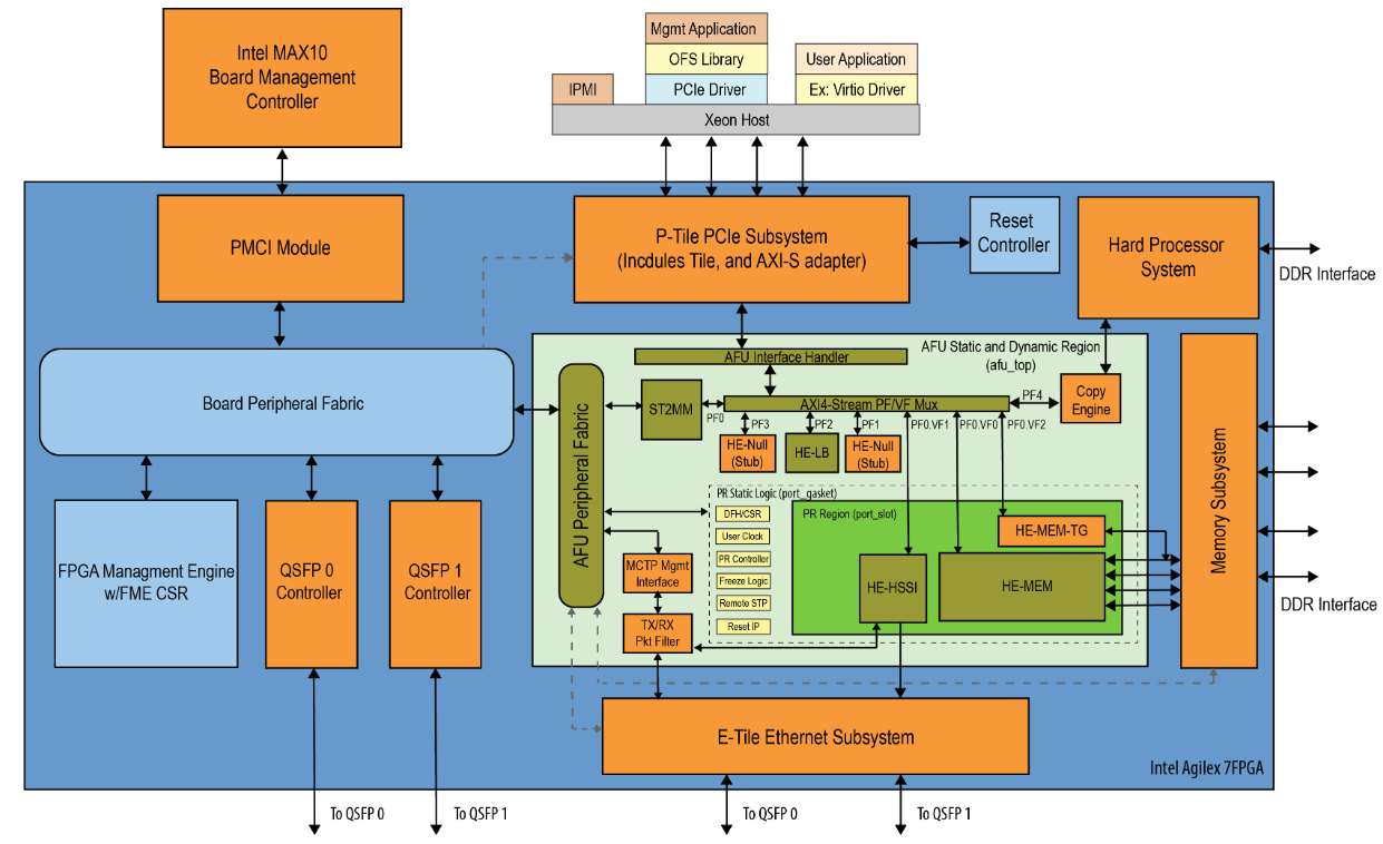
1.2.1.2 Interfaces
The key interfaces in the OFS Agilex PCIe Attach design are listed in the Release Capabilities tables below. They describe the capabilities of the n6001 and n6000 hardware as well as the capabilities of the default OFS Agilex PCIe Attach reference designs targeting the n6001 and the n6000.
Table: Intel® FPGA SmartNIC N6001-PL OFS Release Capabilities
| Interface | Intel® FPGA SmartNIC N6001-PL Hardware Capabilities | n6001 OFS Agilex PCIe Attach Reference Design Implementation |
|---|---|---|
| Host Interface | PCIe Gen4x16 | PCIe Gen4x16 |
| Network Interface | 2 x QSFP-28/56 cages | 2x4x25GbE | 2x1x100GbE | 2x4x10GbE |
| External Memory | 5xDDR4 DIMMs sockets - 40-bits (1 available for HPS) | 4xDDR4 - 2400MHz - 4GB (1Gb x 32) - 32-bits - No ECC1xDDR4 - 2400MHz - 1GB (256Mb x 32 with 256 Mb x8 ECC) - 40-bits - With ECC - For HPS |
Table: Intel® FPGA SmartNIC N6000-PL OFS Release Capabilities
| Interface | Intel® FPGA SmartNIC N6000-PL Hardware Capabilities | n6000 OFS Agilex PCIe Attach Reference Design Implementation |
|---|---|---|
| Host Interface | To Agilex 7: PCIe Gen4x8 To E810: PCIe Gen4x8 | To Agilex 7: PCIe Gen4x8 To E810: PCIe Gen4x8 |
| Network Interface | 2 x QSFP-28/56 cages | 2x2x100GbE |
| External Memory | 5xDDR4 DIMMs sockets - 40-bits (1 available for HPS) | Not enabled by default, but can support: 4xDDR4 - 2400MHz - 4GB (1Gb x 32) - 32-bits - No ECC1xDDR4 - 2400MHz - 1GB (256Mb x 32 with 256 Mb x8 ECC) - 40-bits - With ECC - For HPS |
1.2.1.3 Subsystems
The FIM Subsystems Table describes the Platform Designer IP subsystems used in the OFS Agilex PCIe Attach n6001 FIM.
Table: FIM Subsystems
| Subsystem | User Guide | Document ID |
|---|---|---|
| PCIe Subsystem | PCIe Subsystem Intel FPGA IP User Guide for Intel Agilex OFS | N/A |
| Memory Subsystem | Memory Subsystem Intel FPGA IP User Guide for Intel Agilex OFS | 686148[1] |
| Ethernet Subsystem | Ethernet Subsystem Intel FPGA IP User Guide | 773413[1] |
[1] You must request entitled access to these documents.
1.2.1.4 Host Exercisers
The default AFU workload in the OFS Agilex PCIe Attach n6001/n6000 FIM contains several modules called Host Exercisers which are used to exercise the interfaces on the board. The Host Exerciser Descriptions Table describes these modules.
Table: Host Exerciser Descriptions
| Name | Acronym | Description | OPAE Command |
|---|---|---|---|
| Host Exerciser Loopback | HE-LB | Used to exercise and characterize host to FPGA data transfer. | host_exerciser |
| Host Exerciser Memory | HE_MEM | Used to exercise and characterize host to Memory data transfer. | host_exerciser |
| Host Exerciser Memory Traffic Generator | HE_MEM_TG | Used to exercise and test available memory channels with a configurable traffic pattern. | mem_tg |
| Host Exerciser High Speed Serial Interface | HE-HSSI | n6001: Used to exercise and characterize HSSI interfaces. n6000: Used to pass through data between the E810 to the QSFPs. | hssi |
The host exercisers can be removed from the design at compile-time using command line arguments for the build script.
1.2.1.5 Module Access via APF/BPF
The OFS Agilex PCIe Attach n6001 FIM uses AXI4-Lite interconnect logic named the AFU Peripheral Fabric (APF) and Board Peripheral Fabric (BPF) to access the registers of the various modules in the design. The APF/BPF modules define master/slave interactions, namely between the host software and AFU and board peripherals. The APF Address Map Table describes the address mapping of the APF, followed by the BPF Address Map Table which describes the address mapping of the BPF.
Table: APF Address Map
| Address | Size (Bytes) | Feature |
|---|---|---|
| 0x00000–0x3FFFF | 256K | Board Peripherals (See BPF Address Map table) |
| 0x40000 – 0x4FFFF | 64K | ST2MM |
| 0x50000 – 0x5FFFF | 64K | Reserved |
| 0x60000 – 0x60FFF | 4K | UART |
| 0x61000 – 0x6FFFF | 4K | Reserved |
| 0x70000 – 0x7FFFF | 56K | PR Gasket:4K= PR Gasket DFH, control and status4K= Port DFH4K=User Clock52K=Remote STP |
| 0x80000 – 0x80FFF | 4K | AFU Error Reporting |
Table: BPF Address Map
| Address | Size (Bytes) | Feature |
|---|---|---|
| 0x00000 - 0x0FFFF | 64K | FME |
| 0x10000 - 0x10FFF | 4K | PCIe |
| 0x11000 - 0x11FFF | 4K | Reserved |
| 0x12000 - 0x12FFF | 4K | QSFP0 |
| 0x13000 - 0x13FFF | 4K | QSFP1 |
| 0x14000 - 0x14FFF | 4K | HSSI |
| 0x15000 - 0x15FFF | 4K | EMIF |
| 0x20000 - 0x3FFFF | 128K | PMCI Controller |
1.2.2 Customization Options
OFS is designed to be easily customizable to meet your design needs. The OFS FIM Customization Examples Table lists the general user flows for OFS Agilex PCIe Attach n6001/n6000 FIM development, along with example customizations for each user flow, plus links to step-by-step walkthroughs where available.
Table: OFS FIM Customization Examples
1.3 Development Environment
This section describes the components required for OFS FIM development, and provides a walkthrough for setting up the environment on your development machine.
Note that your development machine may be different than your deployment machine where the FPGA acceleration card is installed. FPGA development work and deployment work can be performed either on the same machine, or on different machines as desired. Please see the Getting Started Guide: OFS for Agilex® 7 PCIe Attach FPGAs (Intel® FPGA SmartNIC N6001-PL/N6000-PL) for instructions on setting up the environment for deployment machines.
1.3.1 Development Tools
The Development Environment Table describes the Best Known Configuration (BKC) for the tools that are required for OFS FIM development.
Table: Development Environment BKC
| Component | Version | Installation Walkthrough |
|---|---|---|
| Operating System | RedHat® Enterprise Linux® (RHEL) 8.6 | N/A |
| Quartus® Prime Pro Edition Software | Quartus Prime Pro Version 23.4 for Linux + Patches 0.17 patch (PCIe) | Section 1.3.1.1 |
| Python | 3.6.8 or later | N/A |
| GCC | 8.5.0 or later | N/A |
| cmake | 3.15 or later | N/A |
| FIM Source Files | ofs-2024.1-1 | Section 1.3.2.1 |
1.3.1.1 Walkthrough: Install Quartus Prime Pro Software
Intel Quartus Prime Pro Version 23.4 is verified to work with the latest OFS release ofs-2024.1-1. However, you have the option to port and verify the release on newer versions of Intel Quartus Prime Pro software.
Use RedHat® Enterprise Linux® (RHEL) 8.6 for compatibility with your development flow and also testing your FIM design in your platform.
Prior to installing Quartus:
-
Ensure you have at least 64 GB of free space for Quartus Prime Pro installation and your development work.
- Intel® recommends that your system be configured to provide virtual memory equal in size or larger than the recommended physical RAM size that is required to process your design.
- The disk space may be significantly more based on the device families included in the install. Prior to installation, the disk space should be enough to hold both zipped tar files and uncompressed installation files. After successful installation, delete the downloaded zipped files and uncompressed zip files to release the disk space.
-
Perform the following steps to satisfy the required dependencies.
$ sudo dnf install -y gcc gcc-c++ make cmake libuuid-devel rpm-build autoconf automake bison boost boost-devel libxml2 libxml2-devel make ncurses grub2 bc csh flex glibc-locale-source libnsl ncurses-compat-libsApply the following configurations.
-
Create the default installation path:
/intelFPGA_pro/ , where is the default path of the Linux workstation, or as set by the system administrator and is your Quartus version number. The installation path must satisfy the following requirements:
- Contain only alphanumeric characters
- No special characters or symbols, such as !$%@^&*<>,
- Only English characters
- No spaces
-
Download your required Quartus Prime Pro Linux version here.
-
Install required Quartus patches. The Quartus patch
.runfiles can be found in the Assets tab on the OFS Release GitHub page. The patches for this release are 0.17 patch (PCIe). -
After running the Quartus Prime Pro installer, set the PATH environment variable to make utilities
quartus,jtagconfig, andquartus_pgmdiscoverable. Edit your bashrc file~/.bashrcto add the following line:export PATH=<Quartus install directory>/quartus/bin:$PATH export PATH=<Quartus install directory>/qsys/bin:$PATHFor example, if the Quartus install directory is /home/intelFPGA_pro/23.4 then the new line is:
-
Verify, Quartus is discoverable by opening a new shell:
1.3.2 FIM Source Files
The source files for the OFS Agilex PCIe Attach FIM are provided in the following repository: https://github.com/OFS/ofs-agx7-pcie-attach/releases/tag/ofs-2024.1-1.
Some essential directories in the repository are described as follows:
ofs-agx7-pcie-attach
|  syn                      // Contains files related to synthesis
|  |  board                     // Contains synthesis files for several cards, including the n6001 and n6000
|  |  |  n6001                  // Contains synthesis files for n6001 and n6000
|  |  |  |  setup                       // Contains setup files, including pin constraints and location constraints
|  |  |  |  syn_top                     // Contains Quartus project files
|  verification             // Contains files for UVM testing
|  ipss                     // Contains files for IP Sub-Systems
|  |  qsfp                      // Contains source files for QSFP Sub-System
|  |  hssi                      // Contains source files for HSSI Sub-System
|  |  pmci                      // Contains source files for PMCI Sub-System (not used in F-Tile FIM)
|  |  pcie                      // Contains source files for PCIe Sub-System
|  |  mem                       // Contains source files for Memory Sub-System
|  sim                      // Contains simulation files
|  |  unit_test                 // Contains files for all unit tests
|  |  |  scripts                    // Contains script to run regression unit tests
|  license                  // Contains Quartus patch
|  ofs-common               // Contains files which are common across OFS platforms
|  |  verification              // Contains common UVM files
|  |  scripts                   // Contains common scripts
|  |  |  common
|  |  |  |  syn                         // Contains common scripts for synthesis, including build script
|  |  |  |  sim                         // Contains common scripts for simulation
|  |  tools                     // Contains common tools files
|  |  |  mk_csr_module              // Contains common files for CSR modules
|  |  |  fabric_generation          // Contains common files for APF/BPF fabric generation
|  |  |  ofss_config                // Contains common files for OFSS configuration tool
|  |  |  |  ip_params                   // Contains default IP parameters for certain Sub-Systems when using OFSS
|  |  src                       // Contains common source files, including host exercisers
|  tools                    //
|  |  ofss_config               // Contains top level OFSS files for each pre-made board configuration
|  |  |  hssi                       // Contains OFSS files for Ethernet-SS configuraiton
|  |  |  memory                     // Contains OFSS files for Memory-SS configuration
|  |  |  pcie                       // Contains OFSS files for PCIe-SS configuration
|  |  |  iopll                      // Contains OFSS files for IOPLL configuration
|  src                      // Contains source files for Agilex PCIe Attach FIM
|  |  pd_qsys                   // Contains source files related to APF/BPF fabric
|  |  includes                  // Contains source file header files
|  |  top                       // Contains top-level source files, including design top module
|  |  afu_top                   // Contains top-level source files for AFU
1.3.2.1 Walkthrough: Clone FIM Repository
Perform the following steps to clone the OFS Agilex® 7 PCIe Attach FIM Repository:
-
Create a new directory to use as a clean starting point to store the retrieved files.
-
Clone GitHub repository using the HTTPS git method
-
Check out the correct tag of the repository
-
Ensure that
ofs-commonhas been cloned as wellExample output:
1.3.3 Environment Variables
The OFS FIM compilation and simulation scripts require certain environment variables be set prior to execution.
1.3.3.1 Walkthrough: Set Development Environment Variables
Perform the following steps to set the required environment variables. These environment variables must be set prior to simulation or compilation tasks so it is recommended that you create a script to set these variables.
-
Navigate to the top level directory of the cloned OFS FIM repository.
-
Set project variables
-
Set variables based on your development environment
# Set proxies if required for your server export http_proxy=<YOUR_HTTP_PROXY> export https_proxy=<YOUR_HTTPS_PROXY> export ftp_proxy=<YOUR_FTP_PROXY> export socks_proxy=<YOUR_SOCKS_PROXY> export no_proxy=<YOUR_NO_PROXY> # Set Quartus license path export LM_LICENSE_FILE=<YOUR_LM_LICENSE_FILE> # Set Synopsys License path (if using Synopsys for simulation) export DW_LICENSE_FILE=<YOUR_DW_LICENSE_FILE> export SNPSLMD_LICENSE_FILE=<YOUR_SNPSLMD_LICENSE_FILE> # Set Quartus Installation Directory - e.g. $QUARTUS_ROOTDIR/bin contains Quartus executables export QUARTUS_ROOTDIR=<YOUR_QUARTUS_INSTALLATION_DIRECTORY> # Set the Tools Directory - e.g. $TOOLS_LOCATION contains the 'synopsys' directory if you are using Synopsys. Refer to the $VCS_HOME variable for an example. export TOOLS_LOCATION=<YOUR_TOOLS_LOCATION> -
Set generic environment variables
# Set Work directory
export WORKDIR=$OFS_ROOTDIR

# Set Quartus Tools variables
export QUARTUS_HOME=$QUARTUS_ROOTDIR
export QUARTUS_INSTALL_DIR=$QUARTUS_ROOTDIR
export QUARTUS_ROOTDIR_OVERRIDE=$QUARTUS_ROOTDIR
export QUARTUS_VER_AC=$QUARTUS_ROOTDIR
export IP_ROOTDIR=$QUARTUS_ROOTDIR/../ip
export IMPORT_IP_ROOTDIR=$IP_ROOTDIR
export QSYS_ROOTDIR=$QUARTUS_ROOTDIR/../qsys/bin

# Set Verification Tools variables (if running simulations)
export DESIGNWARE_HOME=$TOOLS_LOCATION/synopsys/vip_common/vip_Q-2020.03A
export UVM_HOME=$TOOLS_LOCATION/synopsys/vcsmx/S-2021.09-SP1/linux64/rhel/etc/uvm
export VCS_HOME=$TOOLS_LOCATION/synopsys/vcsmx/S-2021.09-SP1/linux64/rhel
export MTI_HOME=$QUARTUS_ROOTDIR/../questa_fse
export VERDIR=$OFS_ROOTDIR/verification
export VIPDIR=$VERDIR

# Set OPAE variables
export OPAE_SDK_REPO_BRANCH=release/2.12.0

# Set PATH to include compilation and simulation tools
export PATH=$QUARTUS_HOME/bin:$QUARTUS_HOME/../qsys/bin:$QUARTUS_HOME/sopc_builder/bin/:$IOFS_BUILD_ROOT/opae-sdk/install-opae-sdk/bin:$MTI_HOME/linux_x86_64/:$MTI_HOME/bin/:$DESIGNWARE_HOME/bin:$VCS_HOME/bin:$PATH
1.3.4 Walkthrough: Set Up Development Environment
This walkthrough guides you through the process of setting up your development environment in preparation for FIM development. This flow only needs to be done once on your development machine.
-
Ensure that Quartus Prime Pro Version 23.4 for Linux with Agilex® 7 FPGA device support is installed on your development machine. Refer to the Install Quartus Prime Pro Software section for step-by-step installation instructions.
- Verify version number
Example Output:
- Verify version number
-
Ensure that all support tools are installed on your development machine, and that they meet the version requirements.
-
Python 3.6.8 or later
-
Verify version number
Example Output:
-
-
GCC 8.5.0 or later
-
Verify version number
Example output:
-
-
cmake 3.15 or later
-
Verify version number
Example output:
-
-
-
Clone the ofs-agx7-pcie-attach repository. Refer to the Clone FIM Repository section for step-by-step instructions.
-
Install UART IP license patch
.02.-
Navigate to the
licensedirectory -
Install Patch 0.02
-
-
Install Quartus Patches 0.17 patch (PCIe). All required patches are provided in the Assets of the OFS FIM Release: https://github.com/OFS/ofs-agx7-pcie-attach/releases/tag/ofs-2024.1-1
-
Extract and unzip the
patch-agx7-2024-1.tar.gzfile. -
Run each patch
.runfile. As an example:
-
-
Verify that patches have been installed correctly. They should be listed in the output of the following command.
-
Set required environment variables. Refer to the Set Development Environment Variables section for step-by-step instructions.
This concludes the walkthrough for setting up your development environment. At this point you are ready to begin FIM development.
2. FIM Compilation
This section describes the process of compiling OFS FIM designs using the provided build scripts. It contains two main sections:
- Compilation Theory - Describes the theory behind FIM compilation
- Compilation Flows - Describes the process of compiling a FIM
The walkthroughs provided in this section are:
2.1 Compilation Theory
This section describes the theory behind FIM compilation.
2.1.1 FIM Build Script
The OFS Common Repository contains a script named build_top.sh which is used to build OFS FIM designs and generate output files that can be programmed to the board. After cloning the OFS FIM repository (with the ofs-common repository included), the build script can be found in the following location:
The usage of the build_top.sh script is as follows:
build_top.sh [-k] [-p] [-e] [--stage=<action>] [--ofss=<ip_config>] <build_target>[:<fim_options>] [<work_dir_name>]
| Field | Options | Description | Requirement |
|---|---|---|---|
-k |
None | Keep. Preserves and rebuilds within an existing work tree instead of overwriting it. | Optional |
-p |
None | When set, and if the FIM supports partial reconfiguration, a PR template tree is generated at the end of the FIM build. The PR template tree is located in the top of the work directory but is relocatable and uses only relative paths. See $OFS_ROOTDIR/syn/common/scripts generate_pr_release.sh for details. | Optional |
-e |
None | Run only Quartus analysis and elaboration. It completes the setup stage, passes -end synthesis to the Quartus compilation flow and exits without running the finish stage. |
Optional |
--stage |
all | setup | compile | finish |
Controls which portion of the OFS build is run. - all: Run all build stages (default) - setup: Initialize a project in the work directory - compile: Run the Quartus compilation flow on a project that was already initialized with setup - finish: Complete OFS post-compilation tasks, such as generating flash images and, if -p is set, generating a release. |
Optional |
--ofss |
<ip_config> |
Used to modify IP, such as the PCIe SS, using .ofss configuration files. This parameter is consumed during the setup stage and IP is updated only inside the work tree. More than one .ofss file may be passed to the --ofss switch by concatenating them separated by commas. For example: --ofss config_a.ofss,config_b.ofss. |
Optional |
<build_target> |
n6000 | n6001 | fseries-dk | iseries-dk |
Specifies which board is being targeted. | Required |
<fim_options> |
flat | null_he_lb | null_he_hssi | null_he_mem | null_he_mem_tg | no_hssi |
Used to change how the FIM is built. • flat - Compiles a flat design (no PR assignments). This is useful for bringing up the design on a new board without dealing with PR complexity. • null_he_lb - Replaces the Host Exerciser Loopback (HE_LBK) with he_null. • null_he_hssi - Replaces the Host Exerciser HSSI (HE_HSSI) with he_null. • null_he_mem - Replaces the Host Exerciser Memory (HE_MEM) with he_null. • null_he_mem_tg - Replaces the Host Exerciser Memory Traffic Generator with he_null. • no_hssi - Removes the HSSI-SS from the FIM. More than one FIM option may be passed included in the <fim_options> list by concatenating them separated by commas. For example: <build_target>:flat,null_he_lb,null_he_hssi |
Optional |
<work_dir_name> |
String | Specifies the name of the work directory in which the FIM will be built. If not specified, the default target is $OFS_ROOTDIR/work |
Optional |
Refer to Compile OFS FIM which provides step-by-step instructions for running the build_top.sh script with some of the different available options.
2.1.1.1 Build Work Directory
The build script copies source files from the existing cloned repository into the specified work directory, which are then used for compilation. As such, any changes made in the base source files will be included in all subsequent builds, unless the -k option is used, in which case an existing work directories files are used as-is. Likewise, any changes made in a work directory is only applied to that work directory, and will not be updated in the base repository by default. When using OFSS files to modify the design, the build script will create a work directory and make the modifications in the work directory.
2.1.1.2 Null Host Exercisers
An HE_NULL FIM refers to a design with one, some, or all of the Host Exercisers replaced by he_null blocks. The he_null is a minimal block with CSRs that responds to PCIe MMIO requests in order to keep PCIe alive. You may use any of the build flows (flat, in-tree, out-of-tree) with the HE_NULL compile options. The HE_NULL compile options are as follows:
null_he_lb- Replaces the Host Exerciser Loopback (HE_LBK) withhe_nullnull_he_hssi- Replaces the Host Exerciser HSSI (HE_HSSI) withhe_nullnull_he_mem- Replaces the Host Exerciser Memory (HE_MEM) withhe_nullnull_he_mem_tg- Replaces the Host Exerciser Memory Traffic Generator withhe_null
The Compile OFS FIM section gives step-by-step instructions for this flow.
2.1.2 OFSS File Usage
The OFS FIM build script can use OFSS files to easily customize design IP prior to compilation using preset configurations. The OFSS files specify certain parameters for different IPs. Using OFSS is provided as a convenience feature for building FIMs. The Provided OFSS Files table below describes the pre-made OFSS files for the n6001 that can be found in the $OFS_ROOTDIR/tools/ofss_config directory. Only the OFSS files listed in this table are compatible with the n6001 In order to compile an n6001 FIM, you must supply OFSS files corresponding to each IP that is present in your design.
Table: Provided OFSS Files
| OFSS File Name | Location | Type | Description | Supported Board |
|---|---|---|---|---|
n6001.ofss |
$OFS_ROOTDIR/tools/ofss_config |
Top | Includes the following OFSS files: • n6001_base.ofss • pcie_host.ofss • iopll.ofss • memory.ofss |
N6001 |
n6001_2pf.ofss |
$OFS_ROOTDIR/tools/ofss_config |
Top | Includes the following OFSS files: • n6001_base.ofss • pcie_2pf.ofss • iopll.ofss • memory.ofss |
N6001 |
n6001_1pf_1vf.ofss |
$OFS_ROOTDIR/tools/ofss_config |
Top | Includes the following OFSS files: • n6001_base.ofss • pcie_1pf_1vf.ofss • iopll.ofss • memory.ofss |
N6001 |
n6000.ofss |
$OFS_ROOTDIR/tools/ofss_config |
Top | Includes the following OFSS files: • n6000_base.ofss • pcie_host_n6000.ofss • iopll_n6000.ofss • hssi_4x100.ofss |
N6000 |
n6001_base.ofss |
$OFS_ROOTDIR/tools/ofss_config |
ofs | Defines certain attributes of the design, including the platform name, device family, fim type, part number, and device ID. | N6001 |
n6000_base.ofss |
$OFS_ROOTDIR/tools/ofss_config |
ofs | Defines certain attributes of the design, including the platform name, device family, fim type, part number, and device ID. | N6000 |
pcie_host.ofss |
$OFS_ROOTDIR/tools/ofss_config/pcie |
pcie | Defines the PCIe Subsystem for the N6001 with the following configuration: • PF0 (3 VFs) • PF1 (0 VFs) • PF2 (0 VFs) • PF3 (0 VFs) • PF4 (0 VFs) | N6001 |
pcie_2pf.ofss |
$OFS_ROOTDIR/tools/ofss_config/pcie |
pcie | Defines the PCIe Subsystem with the following configuration: • PF0 (0 VFs) • PF1 (0 VFs) | N6001 |
pcie_1pf_1vf.ofss |
$OFS_ROOTDIR/tools/ofss_config/pcie |
pcie | Defines the PCIe Subsystem with the following configuration: • PF0 (1 VF) | N6001 |
pcie_host_n6000.ofss |
$OFS_ROOTDIR/tools/ofss_config/pcie |
pcie | Defines the PCIe Subsystem for the N6000 with the following configuration: • PF0 (3 VFs) • PF1 (0 VFs) • PF2 (0 VFs) • PF3 (0 VFs) • PF4 (0 VFs) | N6001 |
iopll.ofss |
$OFS_ROOTDIR/tools/ofss_config/iopll |
iopll | Sets the IOPLL frequency to 470 MHz |
N6001 |
iopll_n6000.ofss |
$OFS_ROOTDIR/tools/ofss_config/iopll |
iopll | Sets the IOPLL frequency to 350 MHz |
N6000 |
memory.ofss |
$OFS_ROOTDIR/tools/ofss_config/memory |
memory | Defines the memory IP preset file to be used during the build as n6001 |
N6001 | N6000 [1] |
hssi_8x25.ofss |
$OFSS_ROOTDIR/tools/ofss_config/hssi |
hssi | Defines the Ethernet-SS IP configuration to be 8x25 GbE | N6001 |
hssi_8x10.ofss |
$OFSS_ROOTDIR/tools/ofss_config/hssi |
hssi | Defines the Ethernet-SS IP configuration to be 8x10 GbE | N6001 |
hssi_2x100.ofss |
$OFSS_ROOTDIR/tools/ofss_config/hssi |
hssi | Defines the Ethernet-SS IP configuration to be 2x100 GbE | N6001 |
hssi_4x100.ofss |
$OFSS_ROOTDIR/tools/ofss_config/hssi |
hssi | Defines the Ethernet-SS IP configuration to be 4x100 GbE | N6000 |
[1] The memory.ofss file can be used for the N6000, however, the default N6000 FIM does not implement the Memory Sub-system. Refer to Section 4.7.2 for step-by-step instructions on how to enable the Memory sub-system
There can typically be three sections contained within an OFSS file.
-
[include]- This section of an OFSS file contains elements separated by a newline, where each element is the path to an OFSS file that is to be included for configuration by the OFSS Configuration Tool. Ensure that any environment variables (e.g.
$OFS_ROOTDIR) is set correctly. The OFSS Config tool uses breadth first search to include all of the specified OFSS files; the ordering of OFSS files does not matter
- This section of an OFSS file contains elements separated by a newline, where each element is the path to an OFSS file that is to be included for configuration by the OFSS Configuration Tool. Ensure that any environment variables (e.g.
-
[ip]- This section of an OFSS file contains a key value pair that allows the OFSS Config tool to determine which IP configuration is being passed in. The currently supported values of IP are
ofs,iopll,pcie,memory, andhssi.
- This section of an OFSS file contains a key value pair that allows the OFSS Config tool to determine which IP configuration is being passed in. The currently supported values of IP are
-
[settings]- This section of an OFSS file contains IP specific settings. Refer to an existing IP OFSS file to see what IP settings are set. For the IP type `ofss``, the settings will be information of the OFS device (platform, family, fim, part #, device_id)
2.1.2.1 Platform OFSS File
The <platform>.ofss file (e.g. $OFS_ROOTDIR/tools/ofss_config/n6001.ofss) is the platform level OFSS wrapper file. This is typically the OFSS file that is provided to the build script. It only contains an include section which lists all other OFSS files that are to be used when the <platform>.ofss file is passed to the build script.
The generic structure of a <platform>.ofss file is as follows:
[include]
<PATH_TO_PLATFORM_BASE_OFSS_FILE>
<PATH_TO_PCIE_OFSS_FILE>
<PATH_TO_IOPLL_OFSS_FILE>
<PATH_TO_MEMORY_OFSS_FILE>
<PATH_TO_HSSI_OFSS_FILE>
2.1.2.2 OFS IP OFSS File
An OFSS file with IP type ofs (e.g. $OFS_ROOTDIR/tools/ofss_config/n6001_base.ofss) contains board specific information for the target board.
Currently supported configuration options for an OFSS file with IP type ofs are described in the OFS IP OFSS File Options table.
Table: OFS IP OFSS File Options
| Section | Parameter | n6001 Default Value | n6000 Default Value |
|---|---|---|---|
[ip] |
type |
ofs |
ofs |
[settings] |
platform |
n6001 |
n6000 |
family |
agilex |
agilex |
|
fim |
base_x16 |
base_x16 |
|
part |
AGFB014R24A2E2V |
AGFB014R24A2E2V |
|
device_id |
6001 |
6000 |
2.1.2.3 PCIe IP OFSS File
An OFSS file with IP type pcie (e.g. $OFS_ROOTDIR/tools/ofss_config/pcie/pcie_host.ofss) is used to configure the PCIe-SS in the FIM.
The PCIe OFSS file has a special section type ([pf*]) which is used to define physical functions (PFs) in the FIM. Each PF has a dedicated section, where the * character is replaced with the PF number. For example, [pf0], [pf1], etc. For reference FIM configurations, you must have at least 1 PF with 1VF, or 2PFs. This is because the PR region cannot be left unconnected. PFs must be consecutive. The PFVF Limitations table describes the supported number of PFs and VFs.
Table: PF/VF Limitations
| Parameter | Value |
|---|---|
| Min # of PFs | 1 (on PF0) |
| Max # of PFs | 8 |
| Min # of VFs | 0 (if 2PFs are used) |
| Max # of VFs | 2000 distributed across all PFs |
Currently supported configuration options for an OFSS file with IP type pcie are described in the PCIe IP OFSS File Options table.
Table: PCIe IP OFSS File Options
| Section | Parameter | Options | Description |
|---|---|---|---|
[ip] |
type |
pcie |
Specifies that this OFSS file configures the PCIe-SS |
[settings] |
output_name |
pcie_ss |
Specifies the output name of the PCIe-SS IP |
preset |
String | OPTIONAL - Specifies the name of a PCIe-SS IP presets file to use when building the FIM. When used, a presets file will take priority over any other parameters set in this OFSS file. | |
[pf*] |
num_vfs |
Integer | Specifies the number of Virtual Functions in the current PF |
bar0_address_width |
Integer | ||
bar4_address_width |
Integer | ||
vf_bar0_address_width |
Integer | ||
ats_cap_enable |
0 | 1 |
||
vf_ats_cap_enable |
0 | 1 |
||
prs_ext_cap_enable |
0 | 1 |
||
pasid_cap_enable |
0 | 1 |
||
pci_type0_vendor_id |
32'h Value | 0x00008086 |
|
pci_type0_device_id |
32'h Value | 0x0000bcce |
|
revision_id |
32'h Value | 0x00000001 |
|
class_code |
32'h Value | 0x00120000 |
|
subsys_vendor_id |
32'h Value | 0x00008086 |
|
subsys_dev_id |
32'h Value | 0x00001771 |
|
sriov_vf_device_id |
32'h Value | 0x0000bccf |
|
exvf_subsysid |
32'h Value | 0x00001771 |
The default values for all PCIe-SS parameters (that are not defined in the PCIe IP OFSS file) are defined in $OFS_ROOTDIR/ofs-common/tools/ofss_config/ip_params/pcie_ss_component_parameters.py. When using a PCIe IP OFSS file during compilation, the PCIe-SS IP that is used will be defined based on the values in the PCIe IP OFSS file plus the parameters defined in pcie_ss_component_parameters.py.
2.1.2.4 IOPLL IP OFSS File
An OFSS file with IP type iopll (e.g. $OFS_ROOTDIR/tools/ofss_config/iopll/iopll.ofss) is used to configure the IOPLL in the FIM.
The IOPLL OFSS file has a special section type ([p_clk]) which is used to define the IOPLL clock frequency.
Currently supported configuration options for an OFSS file with IP type iopll are described in the IOPLL OFSS File Options table.
Table: IOPLL OFSS File Options
| Section | Parameter | Options | Description |
|---|---|---|---|
[ip] |
type |
iopll |
Specifies that this OFSS file configures the IOPLL |
[settings] |
output_name |
sys_pll |
Specifies the output name of the IOPLL. |
instance_name |
iopll_0 |
Specifies the instance name of the IOPLL. | |
[p_clk] |
freq |
Integer: 250 - 470 | Specifies the IOPLL clock frequency in MHz. |
Note: The following frequencies have been tested on reference boards: 350MHz, 400MHz, 470MHz.
2.1.2.5 Memory IP OFSS File
An OFSS file with IP type memory (e.g. $OFS_ROOTDIR/tools/ofss_config/memory/memory.ofss) is used to configure the Memory-SS in the FIM.
The Memory OFSS file specifies a preset value, which selects a presets file (.qprs) to configure the Memory-SS.
Currently supported configuration options for an OFSS file with IP type memory are described in the Memory OFSS File Options table.
Table: Memory OFSS File Options
| Section | Parameter | Options | Description |
|---|---|---|---|
[ip] |
type |
memory |
Specifies that this OFSS file configures the Memory-SS |
[settings] |
output_name |
mem_ss_fm |
Specifies the output name of the Memory-SS. |
preset |
n6001 | String[1] |
Specifies the name of the .qprs presets file that will be used to build the Memory-SS. |
[1] You may generate your own .qprs presets file with a unique name using Quartus.
Memory-SS presets files are stored in the $OFS_ROOTDIR/ipss/mem/qip/presets directory.
2.1.2.6 HSSI IP OFSS File
An OFSS file with IP type hssi (e.g. $OFS_ROOTDIR/tools/ofss_config/hssi/hssi_8x25.ofss) is used to configure the Ethernet-SS in the FIM.
Currently supported configuration options for an OFSS file with IP type hssi are described in the HSSI OFSS File Options table.
Table: HSSI OFSS File Options
| Section | Parameter | Options | Description |
|---|---|---|---|
[ip] |
type |
hssi |
Specifies that this OFSS file configures the Ethernet-SS |
[settings] |
output_name |
hssi_ss |
Specifies the output name of the Ethernet-SS |
num_channels |
Integer | Specifies the number of channels. | |
data_rate |
10GbE | 25GbE | 100GCAUI-4 |
Specifies the data rate | |
preset |
None | String[1] | OPTIONAL - Selects the platform whose preset .qprs file will be used to build the Ethernet-SS. When used, this will overwrite the other settings in this OFSS file. |
[1] You may generate your own .qprs presets file with a unique name using Quartus.
Ethernet-SS presets are stored in $OFS_ROOTDIR/ipss/hssi/qip/hssi_ss/presets directory.
2.1.3 OFS Build Script Outputs
The output files resulting from running the the OFS FIM build_top.sh build script are copied to a single directory during the finish stage of the build script. The path for this directory is:
- For N6001:
$OFS_ROOTDIR/<WORK_DIRECTORY>/syn/board/n6001/syn_top/output_files - For N6000:
$OFS_ROOTDIR/<WORK_DIRECTORY>/syn/board/n6000/syn_top/output_files
The output files include programmable images and compilation reports. The OFS Build Script Output Descriptions table describes the images that are generated by the build script.
Table: OFS Build Script Output Descriptions
| File | Description |
|---|---|
| ofs_top[_hps].bin | This is an intermediate, raw binary file. This intermediate raw binary file is produced by taking the Quartus generated .sof file, and converting it to *.pof using quartus_pfg, then converting the *.pof to *.hexout using quartus_cpf, and finally converting the *.hexout to *.bin using objcopy. Depending on whether the FPGA design contains an HPS block, a different file will be generated. **ofs_top.bin* - Raw binary image of the FPGA generated if there is no HPS present in the design. ofs_top_hps.bin - Raw binary image of the FPGA generated if there is an HPS present in the design. |
| ofs_top_page1.bin | This is the binary of the Factory Image and is the input to PACSign utility to generate ofs_top_page1_unsigned.bin binary image file. This image will carry binary content for the HPS if it is included in the SOF image. |
| ofs_top_page0_factory.bin | This is an input file to PACSign to generate ofs_top_page0_unsigned_factory.bin. |
| ofs_top_page0_unsigned_factory.bin | This is the unsigned PACSign output generated for the Factory Image. |
| ofs_top_page1_user1.bin | This is an input file to PACSign to generate ofs_top_page1_unsigned_user1.bin. This file is created by taking the ofs_top_[hps].bin file and assigning the User1 or appending factory block information. |
| ofs_top_page1_unsigned_user1.bin | This is the unsigned FPGA binary image generated by the PACSign utility for the User1 Image. This file is used to load the FPGA flash User1 Image using the fpgasupdate tool. |
| ofs_top_page2_user2.bin | This is an input file to PACSign to generate ofs_top_page2_unsigned_user2.bin. This file is created by taking the ofs_top_[hps].bin file and assigning the User2 or appending factory block information. |
| ofs_top_page2_unsigned_user2.bin | This is the unsigned FPGA binary image generated by the PACSign utility for the User2 Image. This file is used to load the FPGA flash User2 Image using the fpgasupdate tool. |
| ofs_top_hps.sof | If your design contains an Agilex® 7 FPGA Hard Processor System, then the build assembly process combines the FPGA ofs_top.sof programming file with u-boot-spl-dtb.hex to produce this file. |
2.2 Compilation Flows
This section provides information for using the build script to generate different FIM types. Walkthroughs are provided for each compilation flow. These walkthroughs require that the development environment has been set up as described in the Set Up Development Environment section.
2.2.1 Flat FIM
A flat FIM is compiled such that there is no partial reconfiguration region, and the entire design is built as a flat design. This is useful for compiling new designs without worrying about the complexity introduced by partial reconfiguration. The flat compile removes the PR region and PR IP; thus, you cannot use the -p build flag when using the flat compile setting. Refer to the Compile OFS FIM Section for step-by-step instructions for this flow.
2.2.2 In-Tree PR FIM
An In-Tree PR FIM is the default compilation if no compile flags or compile settings are used. This flow will compile the design with the partial reconfiguration region, but it will not create a relocatable PR directory tree to aid in AFU development. Refer to the Compile OFS FIM Section for step-by-step instructions for this flow.
2.2.3 Out-of-Tree PR FIM
An Out-of-Tree PR FIM will compile the design with the partial reconfiguration region, and will create a relocatable PR directory tree to aid in AFU workload development. This is especially useful if you are developing a FIM to be used by another team developing AFU workloads. This is the recommended build flow in most cases. There are two ways to create the relocatable PR directory tree:
- Run the FIM build script with the
-poption. Refer to the Compile OFS FIM Section for step-by-step instructions for this flow. - Run the
generate_pr_release.shscript after running the FIM build script. Refer to the Walkthrough: Manually Generate OFS Out-Of-Tree PR FIM Section step-by-step instructions for this flow.
In both cases, the generate_pr_release.sh is run to create the relocatable build tree. This script is located at $OFS_ROOTDIR/ofs-common/scripts/common/syn/generate_pr_release.sh. Usage for this script is as follows:
The Generate PR Release Script Options table describes the options for the generate_pr_release.sh script.
Table: Generate PR Release Script Options
| Parameter | Options | Description |
|---|---|---|
<PATH_OF_RELOCATABLE_PR_TREE> |
String | Specifies the location of the relocatable PR directory tree to be created. |
<BOARD_TARGET> |
n6001 | n6000 | fseries-dk | iseries-dk |
Specifies the name of the board target. |
<WORK_DIRECTORY> |
String | Specifies the existing work directory from which the relocatable PR directory tree will be created from. |
After generating the relocatable build tree, it is located in the $OFS_ROOTDIR/<WORK_DIRECTORY>/pr_build_template directory (or the directory you specified if generated separately). The contents of this directory have the following structure:
├── bin
├── ├── afu_synth
├── ├── qar_gen
├── ├── update_pim
├── ├── run.sh
├── ├── build_env_config
├── README
├── hw
├── ├── lib
├── ├── ├── build
├── ├── ├── fme-ifc-id.txt
├── ├── ├── platform
├── ├── ├── fme-platform-class.txt
├── ├── blue_bits
├── ├── ├── ofs_top_hps.sof
└── ├── ├── ofs_top.sof
2.2.5 Walkthrough: Compile OFS FIM
Perform the following steps to compile the OFS Agilex PCIe Attach FIM for n6001 or n6000:
Pre-requisites:
- This walkthrough requires a development environment. Refer to the Set Up Development Environment Section for instructions on setting up a development environment.
Steps:
-
Clone the OFS PCIe Attach FIM repository (or use an existing cloned repository). Refer to the Clone FIM Repository section for step-by-step instructions.
-
Set development environment variables. Refer to the Set Development Environment Variables section for step-by-step instructions.
-
Navigate to the root directory.
-
Run the
build_top.shscript with the desired compile options. Some examples are provided:-
Out-of-Tree PR FIM using OFSS (Standard Flow)
-
N6001
-
N6000
-
-
Flat FIM using OFSS
-
N6001
-
N6000
-
-
In-Tree PR FIM using OFSS
-
N6001
-
N6000
-
-
Flat FIM using OFSS with Host Exercisers Removed
-
N6001
-
N6000
-
-
In-Tree PR FIM using Source
-
N6001
- N6000 - Not supported by default configuration
-
-
-
Once the build script is complete, the build summary should report that the build is complete and passes timing. For example:
2.2.6 Walkthrough: Manually Generate OFS Out-Of-Tree PR FIM
This walkthrough describes how to manually generate an Out-Of-Tree PR FIM. This can be automatically done for you if you run the build script with the -p option. This process is not applicable if you run the build script with the flat option.
Pre-requisites:
- This walkthrough requires a development environment. Refer to the Set Up Development Environment Section for instructions on setting up a development environment.
Steps:
-
Clone the OFS PCIe Attach FIM repository (or use an existing cloned repository). Refer to the Clone FIM Repository section for step-by-step instructions.
-
Set development environment variables. Refer to the Set Development Environment Variables section for step-by-step instructions.
-
Navigate to the root directory.
-
Run the
build_top.shscript with the desired compile options using the n6001 OFSS presets. In order to create the relocatable PR tree, you may not compile with theflatoption. For example:-
N6001
-
N6000
-
-
Run the
generate_pr_release.shscript to create the relocatable PR tree.-
N6001
-
N6000
-
2.2.7 Compilation Seed
You may change the seed which is used by the build script during Quartus compilation to change the starting point of the fitter. Trying different seeds is useful when your design is failing timing by a small amount.
2.2.7.1 Walkthrough: Change the Compilation Seed
Perform the following steps to change the compilation seed for the FIM build.
Pre-requisites:
- This walkthrough requires a development environment. Refer to the Set Up Development Environment Section for instructions on setting up a development environment.
Steps:
-
Clone the OFS PCIe Attach FIM repository (or use an existing cloned repository). Refer to the Clone FIM Repository section for step-by-step instructions.
-
Set development environment variables. Refer to the Set Development Environment Variables section for step-by-step instructions.
-
Edit the
SEEDassignment in the$OFS_ROOTDIR/syn/board/<board_name>/syn_top/ofs_top.qsffile to your desired seed value. The value can be any non-negative integer value.For example, for n6001:
-
Build the FIM. Refer to the Compile OFS FIM section for instructions.
3. FIM Simulation
Unit level simulation of key components in the FIM is provided for verification of the following areas:
- Ethernet
- PCIe
- External Memory
- Core FIM
The Unit Level simulations work with Synopsys VCS/VCSMX or Mentor Graphics Questasim simulators. The scripts to run each unit level simulation are located in $OFS_ROOTDIR/sim/unit_test. Each unit test directory contains a README which describes the test in detail.
3.1 Simulation File Generation
The simulation files must be generated prior to running unit level simulations. The script to generate simulation files is in the following location:
The usage of the gen_sim_files.sh script is as follows:
The Gen Sim Files Script Options table describes the options for the gen_sim_files.sh script.
Table: Gen Sim Files Script Options
| Field | Options | Description | Requirement |
|---|---|---|---|
--ofss |
<ip_config> |
Used to modify IP, such as the PCIe SS, using .ofss configuration files. More than one .ofss file may be passed to the --ofss switch by concatenating them separated by commas. For example: --ofss config_a.ofss,config_b.ofss. |
Platform Dependent[1] |
<build_target> |
n6001 | n6000 | fseries-dk | iseries-dk |
Specifies which board is being targeted. | Required |
<fim_options> |
null_he_lb | null_he_hssi | null_he_mem | null_he_mem_tg |
Used to change how the FIM is built. - null_he_lb - Replaces the Host Exerciser Loopback (HE_LBK) with he_null. - null_he_hssi - Replaces the Host Exerciser HSSI (HE_HSSI) with he_null. - null_he_mem - Replaces the Host Exerciser Memory (HE_MEM) with he_null. - null_he_mem_tg - Replaces the Host Exerciser Memory Traffic Generator with he_null. More than one FIM option may be passed included in the <fim_options> list by concatenating them separated by commas. For example: <build_target>:null_he_lb,null_he_hssi |
Optional |
<device> |
string | Specifies the device ID for the target FPGA. If not specified, the default device is parsed from the QSF file for the project. |
Optional |
<family> |
string | Specifies the family for the target FPGA. If not specified, the default family is parsed from the QSF file for the project. |
Optional |
[1] Using OFSS is required for the N6000, F-Series Development Kit (2xF-Tile), and the I-Series Development Kit (2xR-Tile, 1xF-Tile).
Refer to the Run Individual Unit Level Simulation section for an example of the simulation files generation flow.
When running regression tests, you may use the -g command line argument to generate simulation files; refer to the Run Regression Unit Level Simulation section for step-by-step instructions.
3.2 Individual Unit Tests
Each unit test may be run individually using the run_sim.sh script located in the following directory:
The usage for the run_sim.sh script is as follows:
The Run Sim Script Options table describes the options for the run_sim.sh script.
Table: Run Sim Script Options
| Field | Options | Description |
|---|---|---|
TEST |
String | Specify the name of the test to run, e.g. dfh_walker |
VCSMX |
0 | 1 |
When set, the VCSMX simulator will be used |
MSIM |
0 | 1 |
When set, the QuestaSim simulator will be used |
Note: The default simulator is VCS if neither
VCSMXnorMSIMare set.
The log for a unit test is stored in a transcript file in the simulation directory of the test that was run.
For example, the log for the DFH walker test using VCSMX would be found at:
The simulation waveform database is saved as vcdplus.vpd for post simulation review.
3.2.1 Walkthrough: Run Individual Unit Level Simulation
Perform the following steps to run an individual unit test.
Pre-requisites:
- This walkthrough requires a development environment. Refer to the Set Up Development Environment Section for instructions on setting up a development environment.
Steps:
-
Clone the FIM repository (or use an existing cloned repository). Refer to the Clone FIM Repository section for step-by-step instructions.
-
Set development environment variables. Refer to the Set Development Environment Variables section for step-by-step instructions.
-
Navigate to the simulation directory.
-
Generate the simulation files for the target design.
-
N6001
-
N6000
-
-
Navigate to the common simulation directory
-
Run the desired unit test using your desired simulator
-
Using VCS
-
Using VCSMX
-
Using QuestaSim
-
For example, to run the DFH walker test using VCSMX:
-
-
Once the test is complete, check the output for the simulation results. Review the log for detailed test results.
Example output:
Test status: OK

********************
  Test summary
********************
   test_dfh_walking (id=0) - pass
Test passed!
Assertion count: 0
$finish called from file "/home/ofs-agx7-pcie-attach/sim/unit_test/scripts/../../bfm/rp_bfm_simple/tester.sv", line 210.
$finish at simulation time         356233750000
           V C S   S i m u l a t i o n   R e p o r t
Time: 356233750000 fs
CPU Time:     57.730 seconds;       Data structure size:  47.2Mb
Tue Sep  5 09:44:19 2023
run_sim.sh: USER_DEFINED_SIM_OPTIONS +vcs -l ./transcript
run_sim.sh: run_sim.sh DONE!
3.3 Regression Unit Tests
You may use the regression script regress_run.py to run some or all of the unit tests available with a single command. The regression script is in the following location:
The usage of the regression script is as follows:
regress_run.py [-h] [-l] [-n <num_procs>] [-k <test_package>] [-s <simulator>] [-g] [--ofss <ip_config>] [-b <board_name>] [-e]
The Regression Unit Test Script Options table describes the options for the regress_run.py script.
Table: Regression Unit Test Script Options
| Field | Options | Description |
|---|---|---|
-h | --help |
N/A | Show the help message and exit |
-l | --local |
N/A | Run regression locally |
-n | --n_procs |
Integer | Maximum number of processes/tests to run in parallel when run locally. This has no effect on farm runs. |
-k | --pack |
all | fme | he | hssi | list | mem | pmci |
Test package to run during regression. The "list" option will look for a text file named "list.txt" in the "unit_test" directory for a text list of tests to run (top directory names). The default test package is all. |
-s | --sim |
vcs | vcsmx | msim |
Specifies the simulator used for the regression tests. The default simulator is vcs |
-g | --gen_sim_files |
N/A | Generate simulation files. This only needs to be done once per repo update. This is the equivalent of running the gen_sim_files.sh script. |
-o | --ofss |
<ip_config> |
Used to modify IP, such as the PCIe SS, using .ofss configuration files. More than one .ofss file may be passed to the --ofss switch by concatenating them separated by commas. For example: --ofss config_a.ofss,config_b.ofss. |
-b | --board_name |
n6001 | n6000 | fseries-dk | iseries-dk |
Specifies the board target |
-e | --email_list |
String | Specifies email list to send results to multiple recipients |
The log for each unit test that is run by the regression script is stored in a transcript file in the simulation directory of the test that was run.
For example, the log for the DFH walker test using VCSMX would be found at:
The simulation waveform database is saved as vcdplus.vpd for post simulation review.
3.3.1 Walkthrough: Run Regression Unit Level Simulation
Pre-requisites:
- This walkthrough requires a development environment. Refer to the Set Up Development Environment Section for instructions on setting up a development environment.
Steps:
-
Clone the OFS PCIe Attach FIM repository (or use an existing cloned repository). Refer to the Clone FIM Repository section for step-by-step instructions.
-
Set development environment variables. Refer to the Set Development Environment Variables section for step-by-step instructions.
-
Navigate to the unit test scripts directory.
-
Run regression test with the your desired options. For example, to simulate with the options to generate simulation files, run locally, use 8 processes, run all tests, use VCS simulator, and target the desired board:
-
N6001
-
N6000
-
-
Once all tests are complete, check that the tests have passed.
Example output:
2024-02-15 16:06:47,362: Passing Unit Tests:38/38 >>>>>>>>>>>>>>>>>>>>>>>>>>>>>>>>>>>>>>>>>>>>>>>>>>>>>
2024-02-15 16:06:47,362:    bfm_test:............................. PASS -- Time Elapsed:0:00:56.125802
2024-02-15 16:06:47,362:    csr_test:............................. PASS -- Time Elapsed:0:01:14.072803
2024-02-15 16:06:47,362:    dfh_walker:........................... PASS -- Time Elapsed:0:01:00.565714
2024-02-15 16:06:47,362:    flr:.................................. PASS -- Time Elapsed:0:00:57.453471
2024-02-15 16:06:47,362:    fme_csr_access:....................... PASS -- Time Elapsed:0:00:38.447496
2024-02-15 16:06:47,362:    fme_csr_directed:..................... PASS -- Time Elapsed:0:00:47.593359
2024-02-15 16:06:47,362:    he_lb_test:........................... PASS -- Time Elapsed:0:01:51.150977
2024-02-15 16:06:47,362:    he_mem_lb_test:....................... PASS -- Time Elapsed:0:01:55.940398
2024-02-15 16:06:47,363:    he_null_test:......................... PASS -- Time Elapsed:0:09:34.463979
2024-02-15 16:06:47,363:    hssi_csr_test:........................ PASS -- Time Elapsed:0:07:18.181326
2024-02-15 16:06:47,363:    hssi_kpi_test:........................ PASS -- Time Elapsed:5:45:38.792493
2024-02-15 16:06:47,363:    hssi_test:............................ PASS -- Time Elapsed:5:48:39.722731
2024-02-15 16:06:47,363:    indirect_csr:......................... PASS -- Time Elapsed:0:00:42.677518
2024-02-15 16:06:47,363:    mem_ss_csr_test:...................... PASS -- Time Elapsed:0:00:56.534377
2024-02-15 16:06:47,363:    mem_ss_rst_test:...................... PASS -- Time Elapsed:0:00:55.852359
2024-02-15 16:06:47,363:    mem_tg_test:.......................... PASS -- Time Elapsed:0:00:55.624567
2024-02-15 16:06:47,363:    pcie_ats_basic_test:.................. PASS -- Time Elapsed:0:00:58.659382
2024-02-15 16:06:47,363:    pcie_csr_test:........................ PASS -- Time Elapsed:0:00:58.918341
2024-02-15 16:06:47,363:    pf_vf_access_test:.................... PASS -- Time Elapsed:0:00:57.045204
2024-02-15 16:06:47,363:    pmci_csr_test:........................ PASS -- Time Elapsed:0:01:05.479277
2024-02-15 16:06:47,363:    pmci_mailbox_test:.................... PASS -- Time Elapsed:0:02:34.899524
2024-02-15 16:06:47,363:    pmci_multi_master_test:............... PASS -- Time Elapsed:0:41:09.670790
2024-02-15 16:06:47,363:    pmci_qsfp_telemetry_test:............. PASS -- Time Elapsed:0:40:07.885015
2024-02-15 16:06:47,363:    pmci_rd_default_value_test:........... PASS -- Time Elapsed:0:01:06.944379
2024-02-15 16:06:47,363:    pmci_ro_mailbox_test:................. PASS -- Time Elapsed:0:10:48.580894
2024-02-15 16:06:47,363:    pmci_vdm_b2b_drop_err_scenario_test:.. PASS -- Time Elapsed:0:09:11.081908
2024-02-15 16:06:47,363:    pmci_vdm_len_err_scenario_test:....... PASS -- Time Elapsed:0:14:43.763718
2024-02-15 16:06:47,363:    pmci_vdm_mctp_mmio_b2b_test:.......... PASS -- Time Elapsed:0:01:45.543515
2024-02-15 16:06:47,363:    pmci_vdm_multipkt_error_scenario_test: PASS -- Time Elapsed:1:42:53.665294
2024-02-15 16:06:47,363:    pmci_vdm_multipkt_tlp_err_test:....... PASS -- Time Elapsed:0:21:01.225008
2024-02-15 16:06:47,363:    pmci_vdm_tlp_error_scenario_test:..... PASS -- Time Elapsed:0:20:36.006368
2024-02-15 16:06:47,363:    pmci_vdm_tx_rx_all_random_lpbk_test:.. PASS -- Time Elapsed:0:11:11.355724
2024-02-15 16:06:47,363:    pmci_vdm_tx_rx_all_toggle_test:....... PASS -- Time Elapsed:0:08:15.821700
2024-02-15 16:06:47,363:    pmci_vdm_tx_rx_lpbk_test:............. PASS -- Time Elapsed:0:08:25.528899
2024-02-15 16:06:47,363:    port_gasket_test:..................... PASS -- Time Elapsed:0:00:59.764194
2024-02-15 16:06:47,363:    qsfp_test:............................ PASS -- Time Elapsed:0:07:09.847066
2024-02-15 16:06:47,363:    remote_stp_test:...................... PASS -- Time Elapsed:0:01:01.852028
2024-02-15 16:06:47,363:    uart_csr:............................. PASS -- Time Elapsed:0:01:26.403271
2024-02-15 16:06:47,363: Failing Unit Tests: 0/38 >>>>>>>>>>>>>>>>>>>>>>>>>>>>>>>>>>>>>>>>>>>>>>>>>>>>>
2024-02-15 16:06:47,363: >>>>>>>>>>>>>>>>>>>>>>>>>>>>>>>>>>>>>>>>>>>>>>>>>>>>>>>>>>>>>>>>>>>>>>>>>>>>>>
2024-02-15 16:06:47,363:       Number of Unit test results captured: 38
2024-02-15 16:06:47,363:       Number of Unit test results passing.: 38
2024-02-15 16:06:47,363:       Number of Unit test results failing.:  0
2024-02-15 16:06:47,363:     End Unit regression running at date/time................: 2024-02-15 16:06:47.363814
2024-02-15 16:06:47,363:     Elapsed time for Unit regression run....................: 5:58:50.474807
4. FIM Customization
This section describes how to perform specific customizations of the FIM, and provides step-by-step walkthroughs for these customizations. Each walkthrough can be done independently. These walkthroughs require a development environment. Refer to the Set Up Development Environment Section for instructions on setting up a development environment. The FIM Customization Walkthroughs table lists the walkthroughs that are provided in this section. Some walkthroughs include steps for testing on hardware. Testing on hardware requires that you have a deployment environment set up. Refer to the Getting Started Guide: OFS for Agilex® 7 PCIe Attach FPGAs (Intel® FPGA SmartNIC N6001-PL/N6000-PL) for instructions on setting up a deployment environment.
Table: OFS FIM Customization Examples
4.1 Adding a new module to the FIM
This section provides a information for adding a custom module to the FIM, simulating the new design, compiling the new design, implementing and testing the new design on hardware, and debugging the new design on hardware.
4.1.1 Hello FIM Theory of Operation
If you intend to add a new module to the FIM area, then you will need to inform the host software of the new module. The FIM exposes its functionalities to host software through a set of CSR registers that are mapped to an MMIO region (Memory Mapped IO). This set of CSR registers and their operation is described in FIM MMIO Regions.
See FPGA Device Feature List (DFL) Framework Overview for a description of the software process to read and process the linked list of Device Feature Header (DFH) CSRs within a FPGA.
This example will add a hello_fim module to the design. The Hello FIM example adds a simple DFH register and 64bit scratchpad register connected to the Board Peripheral Fabric (BPF) that can be accessed by the Host. You can use this example as the basis for adding a new feature to your FIM.
For the purposes of this example, the hello_fim module instantiation sets the DFH feature ID (FEAT_ID) to 0x100 which is not currently defined. Using an undefined feature ID will result in no driver being used. Normally, a defined feature ID will be used to associate a specific driver with the FPGA module. Refer to the Device Feature List Feature IDs for a list of DFL feature types and IDs. If you are adding a new module to your design, make sure the Type/ID pair does not conflict with existing Type/ID pairs. You may reserve Type/ID pairs by submitting a pull request at the link above.
The Hello FIM design can be verified by Unit Level simulation, Universal Verification Methodology (UVM) simulation, and running in hardware on the n6001 card. The process for these are described in this section.
4.1.1.1 Hello FIM Board Peripheral Fabric (BPF)
The Hello FIM module will be connected to the Board Peripheral Fabric (BPF), and will be connected such that it can be mastered by the Host. The BPF is an interconnect generated by Platform Designer. The Hello FIM BPF Interface Diagram figure shows the APF/BPF Master/Slave interactions, as well as the added Hello FIM module.
Figure: Hello FIM BPF Interface Diagram
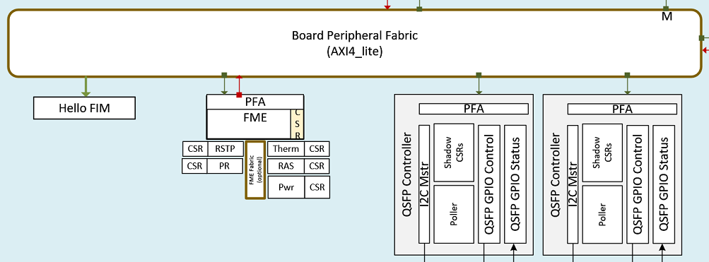
The BPF fabric is defined in $OFS_ROOTDIR/src/pd_qsys/fabric/bpf.txt.
We will add the Hello FIM module to an un-used address space in the MMIO region. The Hello FIM MMIO Address Layout table below shows the MMIO region for the Host with the Hello FIM module added at base address 0x16000.
Table: Hello FIM MMIO Address Layout
| Offset | Feature CSR set |
|---|---|
| 0x00000 | FME AFU |
| 0x10000 | PCIe Interface |
| 0x12000 | QSFP Controller 0 |
| 0x13000 | QSFP Controller 1 |
| 0x14000 | E-Tile Ethernet Interface |
| 0x15000 | EMIF |
| 0x16000 | Hello FIM |
| 0x20000 | PMCI Controller |
| 0x40000 | ST2MM (Streaming to Memory-Mapped) |
| 0x60000 | VUART |
| 0x70000 | PR Control & Status (Port Gasket) |
| 0x71000 | Port CSRs (Port Gasket) |
| 0x72000 | User Clock (Port Gasket) |
| 0x74000 | Remote SignalTap (Port Gasket) |
| 0x80000 | AFU Errors (AFU Interface Handler) |
4.1.1.2 Hello FIM CSR
The Hello FIM CSR will consist of the three registers shown in the Hello FIM CSR table below. The DFH and Hello FIM ID registers are read-only. The Scratchpad register supports read and write accesses.
Table: Hello FIM CSR
| Offset | Attribute | Description | Default Value |
|---|---|---|---|
| 0x016000 | RO | DFH(Device Feature Headers) register | 0x30000006a0000100 |
| 0x016030 | RW | Scrachpad register | 0x0 |
| 0x016038 | RO | Hello FIM ID register | 0x6626070150000034 |
4.1.2 Walkthrough: Add a new module to the OFS FIM
Perform the following steps to add a new module to the OFS FIM that can be accessed by the Host.
Pre-requisites:
- This walkthrough requires a development environment. Refer to the Set Up Development Environment Section for instructions on setting up a development environment.
Steps:
-
Clone the FIM repository (or use an existing cloned repository). Refer to the Clone FIM Repository section for step-by-step instructions.
-
Set development environment variables. Refer to the Set Development Environment Variables section for step-by-step instructions.
-
Make
hello_fimsource directory -
Create
hello_fim_top.svfile.Copy the following code into
hello_fim_top.sv:// *************************************************************************** // INTEL CONFIDENTIAL // // Copyright (C) 2023 Intel Corporation All Rights Reserved. // // The source code contained or described herein and all documents related to // the source code ("Material") are owned by Intel Corporation or its // suppliers or licensors. Title to the Material remains with Intel // Corporation or its suppliers and licensors. The Material contains trade // secrets and proprietary and confidential information of Intel or its // suppliers and licensors. The Material is protected by worldwide copyright // and trade secret laws and treaty provisions. No part of the Material may be // used, copied, reproduced, modified, published, uploaded, posted, // transmitted, distributed, or disclosed in any way without Intel's prior // express written permission. // // No license under any patent, copyright, trade secret or other intellectual // property right is granted to or conferred upon you by disclosure or // delivery of the Materials, either expressly, by implication, inducement, // estoppel or otherwise. Any license under such intellectual property rights // must be express and approved by Intel in writing. // // You will not, and will not allow any third party to modify, adapt, enhance, // disassemble, decompile, reverse engineer, change or create derivative works // from the Software except and only to the extent as specifically required by // mandatory applicable laws or any applicable third party license terms // accompanying the Software. // // ----------------------------------------------------------------------------- // Engineer : // Create Date : September 2023 // Module Name : hello_fim_top.sv // Project : OFS // ----------------------------------------------------------------------------- // // Description: // This is a simple module that implements DFH registers and // AVMM address decoding logic. module hello_fim_top #( parameter ADDR_WIDTH = 12, parameter DATA_WIDTH = 64, parameter bit [11:0] FEAT_ID = 12'h100, parameter bit [3:0] FEAT_VER = 4'h0, parameter bit [23:0] NEXT_DFH_OFFSET = 24'h1000, parameter bit END_OF_LIST = 1'b0 )( input logic clk, input logic reset, // ----------------------------------------------------------- // AXI4LITE Interface // ----------------------------------------------------------- ofs_fim_axi_lite_if.slave csr_lite_if ); import ofs_fim_cfg_pkg::*; import ofs_csr_pkg::*; //------------------------------------- // Signals //------------------------------------- logic [ADDR_WIDTH-1:0] csr_waddr; logic [DATA_WIDTH-1:0] csr_wdata; logic [DATA_WIDTH/8-1:0] csr_wstrb; logic csr_write; logic csr_slv_wready; csr_access_type_t csr_write_type; logic [ADDR_WIDTH-1:0] csr_raddr; logic csr_read; logic csr_read_32b; logic [DATA_WIDTH-1:0] csr_readdata; logic csr_readdata_valid; logic [ADDR_WIDTH-1:0] csr_addr; logic [63:0] com_csr_writedata; logic com_csr_read; logic com_csr_write; logic [63:0] com_csr_readdata; logic com_csr_readdatavalid; logic [5:0] com_csr_address; // AXI-M CSR interfaces ofs_fim_axi_mmio_if #( .AWID_WIDTH (ofs_fim_cfg_pkg::MMIO_TID_WIDTH), .AWADDR_WIDTH (ADDR_WIDTH), .WDATA_WIDTH (ofs_fim_cfg_pkg::MMIO_DATA_WIDTH), .ARID_WIDTH (ofs_fim_cfg_pkg::MMIO_TID_WIDTH), .ARADDR_WIDTH (ADDR_WIDTH), .RDATA_WIDTH (ofs_fim_cfg_pkg::MMIO_DATA_WIDTH) ) csr_if(); // AXI4-lite to AXI-M adapter axi_lite2mmio axi_lite2mmio ( .clk (clk), .rst_n (~reset), .lite_if (csr_lite_if), .mmio_if (csr_if) ); //--------------------------------- // Map AXI write/read request to CSR write/read, // and send the write/read response back //--------------------------------- ofs_fim_axi_csr_slave #( .ADDR_WIDTH (ADDR_WIDTH), .USE_SLV_READY (1'b1) ) csr_slave ( .csr_if (csr_if), .csr_write (csr_write), .csr_waddr (csr_waddr), .csr_write_type (csr_write_type), .csr_wdata (csr_wdata), .csr_wstrb (csr_wstrb), .csr_slv_wready (csr_slv_wready), .csr_read (csr_read), .csr_raddr (csr_raddr), .csr_read_32b (csr_read_32b), .csr_readdata (csr_readdata), .csr_readdata_valid (csr_readdata_valid) ); // Address mapping assign csr_addr = csr_write ? csr_waddr : csr_raddr; assign com_csr_address = csr_addr[5:0]; // byte address assign csr_slv_wready = 1'b1 ; // Write data mapping assign com_csr_writedata = csr_wdata; // Read-Write mapping always_comb begin com_csr_read = 1'b0; com_csr_write = 1'b0; casez (csr_addr[11:6]) 6'h00 : begin // Common CSR com_csr_read = csr_read; com_csr_write = csr_write; end default: begin com_csr_read = 1'b0; com_csr_write = 1'b0; end endcase end // Read data mapping always_comb begin if (com_csr_readdatavalid) begin csr_readdata = com_csr_readdata; csr_readdata_valid = 1'b1; end else begin csr_readdata = '0; csr_readdata_valid = 1'b0; end end hello_fim_com #( .FEAT_ID (FEAT_ID), .FEAT_VER (FEAT_VER), .NEXT_DFH_OFFSET (NEXT_DFH_OFFSET), .END_OF_LIST (END_OF_LIST) ) hello_fim_com_inst ( .clk (clk ), .reset (reset ), .writedata (com_csr_writedata ), .read (com_csr_read ), .write (com_csr_write ), .byteenable (4'hF ), .readdata (com_csr_readdata ), .readdatavalid (com_csr_readdatavalid ), .address (com_csr_address ) ); endmodule -
Create
hello_fim_com.svfile.Copy the following code to
hello_fim_com.sv:module hello_fim_com #( parameter bit [11:0] FEAT_ID = 12'h100, parameter bit [3:0] FEAT_VER = 4'h0, parameter bit [23:0] NEXT_DFH_OFFSET = 24'h1000, parameter bit END_OF_LIST = 1'b0 )( input clk, input reset, input [63:0] writedata, input read, input write, input [3:0] byteenable, output reg [63:0] readdata, output reg readdatavalid, input [5:0] address ); wire reset_n = !reset; reg [63:0] rdata_comb; reg [63:0] scratch_reg; always @(negedge reset_n ,posedge clk) if (!reset_n) readdata[63:0] <= 64'h0; else readdata[63:0] <= rdata_comb[63:0]; always @(negedge reset_n , posedge clk) if (!reset_n) readdatavalid <= 1'b0; else readdatavalid <= read; wire wr = write; wire re = read; wire [5:0] addr = address[5:0]; wire [63:0] din = writedata [63:0]; wire wr_scratch_reg = wr & (addr[5:0] == 6'h30)? byteenable[0]:1'b0; // 64 bit scratch register always @( negedge reset_n, posedge clk) if (!reset_n) begin scratch_reg <= 64'h0; end else begin if (wr_scratch_reg) begin scratch_reg <= din; end end always @ (*) begin rdata_comb = 64'h0000000000000000; if(re) begin case (addr) 6'h00 : begin rdata_comb [11:0] = FEAT_ID ; // dfh_feature_id is reserved or a constant value, a read access gives the reset value rdata_comb [15:12] = FEAT_VER ; // dfh_feature_rev is reserved or a constant value, a read access gives the reset value rdata_comb [39:16] = NEXT_DFH_OFFSET ; // dfh_dfh_ofst is reserved or a constant value, a read access gives the reset value rdata_comb [40] = END_OF_LIST ; //dfh_end_of_list rdata_comb [59:40] = 20'h00000 ; // dfh_rsvd1 is reserved or a constant value, a read access gives the reset value rdata_comb [63:60] = 4'h3 ; // dfh_feat_type is reserved or a constant value, a read access gives the reset value end 6'h30 : begin rdata_comb [63:0] = scratch_reg; end 6'h38 : begin rdata_comb [63:0] = 64'h6626_0701_5000_0034; end default : begin rdata_comb = 64'h0000000000000000; end endcase end end endmodule -
Create
hello_fim_design_files.tclfile.Copy the following code into
hello_fim_design_files.tcl# Copyright 2023 Intel Corporation. # # THIS SOFTWARE MAY CONTAIN PREPRODUCTION CODE AND IS PROVIDED BY THE # COPYRIGHT HOLDERS AND CONTRIBUTORS "AS IS" AND ANY EXPRESS OR IMPLIED # WARRANTIES, INCLUDING, BUT NOT LIMITED TO, THE IMPLIED WARRANTIES OF # MERCHANTABILITY AND FITNESS FOR A PARTICULAR PURPOSE ARE # DISCLAIMED. IN NO EVENT SHALL THE COPYRIGHT HOLDER OR CONTRIBUTORS BE # LIABLE FOR ANY DIRECT, INDIRECT, INCIDENTAL, SPECIAL, EXEMPLARY, OR # CONSEQUENTIAL DAMAGES (INCLUDING, BUT NOT LIMITED TO, PROCUREMENT OF # SUBSTITUTE GOODS OR SERVICES; LOSS OF USE, DATA, OR PROFITS; OR # BUSINESS INTERRUPTION) HOWEVER CAUSED AND ON ANY THEORY OF LIABILITY, # WHETHER IN CONTRACT, STRICT LIABILITY, OR TORT (INCLUDING NEGLIGENCE # OR OTHERWISE) ARISING IN ANY WAY OUT OF THE USE OF THIS SOFTWARE, # EVEN IF ADVISED OF THE POSSIBILITY OF SUCH DAMAGE. # # Hello FIM Files #-------------------- set_global_assignment -name SYSTEMVERILOG_FILE $::env(BUILD_ROOT_REL)/src/hello_fim/hello_fim_com.sv set_global_assignment -name SYSTEMVERILOG_FILE $::env(BUILD_ROOT_REL)/src/hello_fim/hello_fim_top.sv -
Modify
ofs_top.qsffor the target board to include Hello FIM module-
N6001
-
N6000
Add the following line:
-
-
Modify
ofs_top_sources.tclfor the target board to include Hello FIM design files-
N6001
-
N6000
Add the following line:
-
-
Modify
fabric_design_files.tclto include BPF Hello FIM Slave IP.Add the following line:
-
Modify
fabric_width_pkg.svto add Hello FIM slave information and update EMIF slave next offset.-
Open
fabric_width_pkg.sv -
Add/modify the following lines:
-
-
Modify
top.svto support the Hello FIM module.-
Open
top.sv -
Add
bpf_hello_fim_slv_ifto AXI interfaces -
Add Hello FIM instantiation
//******************************* // Hello FIM Subsystem //******************************* `ifdef INCLUDE_HELLO_FIM hello_fim_top #( .ADDR_WIDTH (fabric_width_pkg::bpf_hello_fim_slv_address_width), .DATA_WIDTH (64), .FEAT_ID (12'h100), .FEAT_VER (4'h0), .NEXT_DFH_OFFSET (fabric_width_pkg::bpf_hello_fim_slv_next_dfh_offset), .END_OF_LIST (fabric_width_pkg::bpf_hello_fim_slv_eol) ) hello_fim_top_inst ( .clk (clk_csr), .reset(~rst_n_csr), .csr_lite_if (bpf_hello_fim_slv_if) ); `else dummy_csr #( .FEAT_ID (12'h100), .FEAT_VER (4'h0), .NEXT_DFH_OFFSET (fabric_width_pkg::bpf_hello_fim_slv_next_dfh_offset), .END_OF_LIST (fabric_width_pkg::bpf_hello_fim_slv_eol) ) hello_fim_dummy ( .clk (clk_csr), .rst_n (rst_n_csr), .csr_lite_if (bpf_hello_fim_slv_if) ); `endif -
Add interfaces for Hello FIM slv to bpf instantiation
bpf bpf (
...
  .bpf_hello_fim_slv_awaddr   (bpf_hello_fim_slv_if.awaddr  ),
  .bpf_hello_fim_slv_awprot   (bpf_hello_fim_slv_if.awprot  ),
  .bpf_hello_fim_slv_awvalid  (bpf_hello_fim_slv_if.awvalid ),
  .bpf_hello_fim_slv_awready  (bpf_hello_fim_slv_if.awready ),
  .bpf_hello_fim_slv_wdata    (bpf_hello_fim_slv_if.wdata   ),
  .bpf_hello_fim_slv_wstrb    (bpf_hello_fim_slv_if.wstrb   ),
  .bpf_hello_fim_slv_wvalid   (bpf_hello_fim_slv_if.wvalid  ),
  .bpf_hello_fim_slv_wready   (bpf_hello_fim_slv_if.wready  ),
  .bpf_hello_fim_slv_bresp    (bpf_hello_fim_slv_if.bresp   ),
  .bpf_hello_fim_slv_bvalid   (bpf_hello_fim_slv_if.bvalid  ),
  .bpf_hello_fim_slv_bready   (bpf_hello_fim_slv_if.bready  ),
  .bpf_hello_fim_slv_araddr   (bpf_hello_fim_slv_if.araddr  ),
  .bpf_hello_fim_slv_arprot   (bpf_hello_fim_slv_if.arprot  ),
  .bpf_hello_fim_slv_arvalid  (bpf_hello_fim_slv_if.arvalid ),
  .bpf_hello_fim_slv_arready  (bpf_hello_fim_slv_if.arready ),
  .bpf_hello_fim_slv_rdata    (bpf_hello_fim_slv_if.rdata   ),
  .bpf_hello_fim_slv_rresp    (bpf_hello_fim_slv_if.rresp   ),
  .bpf_hello_fim_slv_rvalid   (bpf_hello_fim_slv_if.rvalid  ),
  .bpf_hello_fim_slv_rready   (bpf_hello_fim_slv_if.rready  ),
...
);
-
-
Modify
$OFS_ROOTDIR/src/pd_qsys/fabric/bpf.txtto add thehello_fimmodule as a slave to theapf. -
Execute helper script to generate BPF design files
-
Once the script completes, the following new IP is created:
$OFS_ROOTDIR/src/pd_qsys/fabric/ip/bpf/bpf_hello_fim_slv.ip. -
[OPTIONAL] You may verify the BPF changes have been made correctly by opening
bpf.qsysto analyze the BPF.-
Navigate to the
$OFS_ROOTDIR/src/pd_qsys/fabricdirectory. -
Open the
bpf.qsysfile.-
N6001
-
N6000
-
-
Find the
bpf_hello_fim_slvinstance:
-
-
Compile the Hello FIM design:
-
Return to the OFS root directory.
-
Call the
build_top.shscript for the target board.-
N6001
-
N6000
-
-
4.1.3 Walkthrough: Modify and run unit tests for a FIM that has a new module
Perform the following steps to modify the unit test files to support a FIM that has had a new module added to it.
Pre-requisites:
- This walkthrough requires a development environment. Refer to the Set Up Development Environment Section for instructions on setting up a development environment.
Steps:
-
This walkthrough uses a FIM design that has had a Hello FIM module added to it. Refer to the Add a new module to the OFS FIM section for step-by-step instructions for creating a Hello FIM design. You do not need to compile the design in order to simulate.
-
Set development environment variables. Refer to the Set Development Environment Variables section for step-by-step instructions.
-
Modify
$OFS_ROOTDIR/sim/unit_test/dfh_walker/test_csr_defs.sv-
Add
HELLO_FIM_IDXentry tot_dfh_idxenumeration.... typedef enum { FME_DFH_IDX, THERM_MNGM_DFH_IDX, GLBL_PERF_DFH_IDX, GLBL_ERROR_DFH_IDX, QSFP0_DFH_IDX, QSFP1_DFH_IDX, HSSI_DFH_IDX, EMIF_DFH_IDX, HELLO_FIM_DFH_IDX, // New PMCI_DFH_IDX, ST2MM_DFH_IDX, VUART_DFH_IDX, PG_PR_DFH_IDX, PG_PORT_DFH_IDX, PG_USER_CLK_DFH_IDX, PG_REMOTE_STP_DFH_IDX, AFU_ERR_DFH_IDX, MAX_DFH_IDX } t_dfh_idx; ... -
Add
HELLO_FIM_DFHtoget_dfh_namesfunction. -
Add expected DFH value for Hello FIM to the
get_dfh_valuesfunction.... function automatic [MAX_DFH_IDX-1:0][63:0] get_dfh_values(); ... dfh_values[PMCI_DFH_IDX] = 64'h3_00000_xxxxxx_1012; dfh_values[PMCI_DFH_IDX][39:16] = fabric_width_pkg::bpf_pmci_slv_next_dfh_offset; dfh_values[HELLO_FIM_DFH_IDX] = 64'h3_00000_xxxxxx_0100; // New dfh_values[HELLO_FIM_DFH_IDX][39:16] = fabric_width_pkg::bpf_hello_fim_slv_next_dfh_offset; // New dfh_values[ST2MM_DFH_IDX] = 64'h3_00000_xxxxxx_0014; dfh_values[ST2MM_DFH_IDX][39:16] = fabric_width_pkg::apf_st2mm_slv_next_dfh_offset; ... return dfh_values; ...
-
-
Generate simulation files:
-
Navigate to the sim directory.
-
Run the
gen_sim_files.shscript.-
N6001
-
N6000
-
-
-
Run DFH Walker Simulation
-
Verify that the test passes, and that the output shows the Hello FIM in the DFH sequence.
********************************************
 Running TEST(0) : test_dfh_walking
********************************************
...

READ64: address=0x00015000 bar=0 vf_active=0 pfn=0 vfn=0

   ** Sending TLP packets **
   ** Waiting for ack **
   READDATA: 0x3000000010001009

EMIF_DFH
   Address   (0x15000)
   DFH value (0x3000000010001009)

READ64: address=0x00016000 bar=0 vf_active=0 pfn=0 vfn=0

   ** Sending TLP packets **
   ** Waiting for ack **
   READDATA: 0x30000000a0000100

HELLO_FIM_DFH
   Address   (0x16000)
   DFH value (0x30000000a0000100)

READ64: address=0x00020000 bar=0 vf_active=0 pfn=0 vfn=0

   ** Sending TLP packets **
   ** Waiting for ack **
   READDATA: 0x3000000200001012

PMCI_DFH
   Address   (0x20000)
   DFH value (0x3000000200001012)

...

Test status: OK

********************
  Test summary
********************
   test_dfh_walking (id=0) - pass
Test passed!
Assertion count: 0
$finish called from file "/home/ofs-agx7-pcie-attach/sim/unit_test/scripts/../../bfm/rp_bfm_simple/tester.sv", line 210.
$finish at simulation time         356791250000
           V C S   S i m u l a t i o n   R e p o r t
Time: 356791250000 fs
CPU Time:     61.560 seconds;       Data structure size:  47.4Mb
Tue Aug 15 16:29:45 2023
run_sim.sh: USER_DEFINED_SIM_OPTIONS +vcs -l ./transcript
run_sim.sh: run_sim.sh DONE!
4.1.4 Walkthrough: Modify and run UVM tests for a FIM that has a new module
Perform the following steps to modify the UVM simulation files to support the Hello FIM design.
Pre-requisites:
- This walkthrough requires a development environment. Refer to the Set Up Development Environment Section for instructions on setting up a development environment.
- This walkthrough uses a FIM design that has had a Hello FIM module added to it. Refer to the Add a new module to the OFS FIM section for step-by-step instructions for creating a Hello FIM design. You do not need to compile the design in order to simulate.
Steps:
-
Modify
$OFS_ROOTDIR/verification/tests/sequences/dfh_walking_seq.svh-
Modify the
dfh_offset_arrayto insert the Hello FIM atdfh_offset_array[8].dfh_offset_array = new[17]; dfh_offset_array[0] = tb_cfg0.PF0_BAR0; // FME_DFH 0x8000_0000 dfh_offset_array[1] = dfh_offset_array[0] + 64'h0_1000; // THERM_MNGM_DFH 0x8000_1000 dfh_offset_array[2] = dfh_offset_array[1] + 64'h0_2000; // GLBL_PERF_DFH 0x8000_3000 dfh_offset_array[3] = dfh_offset_array[2] + 64'h0_1000; // GLBL_ERROR_DFH 0x8000_4000 dfh_offset_array[4] = dfh_offset_array[3] + 64'h0_E000; // QSFP0_DFH 0x8001_2000 dfh_offset_array[5] = dfh_offset_array[4] + 64'h0_1000; // QSFP1_DFH 0x8001_3000 dfh_offset_array[6] = dfh_offset_array[5] + 64'h0_1000; // HSSI_DFH 0x8001_4000 dfh_offset_array[7] = dfh_offset_array[6] + 64'h0_1000; // EMIF_DFH 0x8001_5000 dfh_offset_array[8] = dfh_offset_array[7] + 64'h0_1000; // HELLO_FIM_DFH 0x8001_6000 dfh_offset_array[9] = dfh_offset_array[8] + 64'h0_A000; // PMCI_DFH 0x8002_0000 dfh_offset_array[10] = dfh_offset_array[9] + 64'h2_0000; // ST2MM_DFH 0x8004_0000 dfh_offset_array[11] = dfh_offset_array[10] + 64'h2_0000; // VUART_DFH 0x8006_0000 dfh_offset_array[12] = dfh_offset_array[11] + 64'h1_0000; // PG_PR_DFH_IDX 0x8007_0000 dfh_offset_array[13] = dfh_offset_array[12] + 64'h0_1000; // PG_PORT_DFH_IDX 0x8007_1000 dfh_offset_array[14] = dfh_offset_array[13] + 64'h0_1000; // PG_USER_CLK_DFH_IDX 0x8007_2000 dfh_offset_array[15] = dfh_offset_array[14] + 64'h0_1000; // PG_REMOTE_STP_DFH_IDX 0x8007_3000 dfh_offset_array[16] = dfh_offset_array[15] + 64'h0_D000; // PG_AFU_ERR_DFH_IDX 0x8008_0000
-
-
Modify `$OFS_ROOTDIR/verification/tests/sequences/mmio_seq.svh``
-
Add test code related to the Hello FIM. This code will verify the scratchpad register at 0x16030 and read only the register at 0x16038.
// HELLO_FIM_Scratchpad 64 bit access
`uvm_info(get_name(), $psprintf("////Accessing PF0 HELLO_FIM_Scratchpad Register %0h+'h16030////", tb_cfg0.PF0_BAR0), UVM_LOW)

assert(std::randomize(wdata));
addr = tb_cfg0.PF0_BAR0+'h1_6000+'h30;

mmio_write64(.addr_(addr), .data_(wdata));
mmio_read64 (.addr_(addr), .data_(rdata));

if(wdata !== rdata)
    `uvm_error(get_name(), $psprintf("Data mismatch 64! Addr = %0h, Exp = %0h, Act = %0h", addr, wdata, rdata))
else
    `uvm_info(get_name(), $psprintf("Data match 64! addr = %0h, data = %0h", addr, rdata), UVM_LOW)

addr = tb_cfg0.PF0_BAR0+'h1_6000+'h38;
wdata = 64'h6626_0701_5000_0034;
mmio_read64 (.addr_(addr), .data_(rdata));
if(wdata !== rdata)
    `uvm_error(get_name(), $psprintf("Data mismatch 64! Addr = %0h, Exp = %0h, Act = %0h", addr, wdata, rdata))
else
    `uvm_info(get_name(), $psprintf("Data match 64! addr = %0h, data = %0h", addr, rdata), UVM_LOW)
Note: uvm_info and uvm_error statements will put a message into log file.
-
-
Modify
$OFS_ROOTDIR/verification/scripts/Makefile_VCS.mk-
Add
INCLUDE_HELLO_FIMdefine option to enable Hello FIM on UVM
-
-
Re-generate the UVM files
-
Navigate to the verification scripts directory
-
Clean the output of previous builds
-
Compile the IP files
-
N6001
-
N6000
Note: The default N6000 shell has the Memory Sub-System removed, so the
DISABLE_EMIFflag must be set when compiling IP files for UVM simulation. If you add the Memory Sub-System back to the shell design, you must run this command without theDISABLE_EMIFflag.
-
-
Build the RTL and Test Benches
-
N6001
-
N6000
Note: The default N6000 shell has the Memory Sub-System removed, so the
DISABLE_EMIFflag must be set when building the RTL and Test Benches for UVM simulation. If you add the Memory Sub-System back to the shell design, you must run this command without theDISABLE_EMIFflag.
-
-
-
Run the UVM DFH Walker Simulation
-
N6001
-
N6000
Note: The default N6000 shell has the Memory Sub-System removed, so the
DISABLE_EMIFflag must be set when running UVM simulations. If you add the Memory Sub-System back to the shell design, you must run this command without theDISABLE_EMIFflag.
-
-
Verify the DFH Walker test results
-
The output logs are stored in the $VERDIR/sim/dfh_walking_test directory. The main files to note are described in Table 5-3:
Table 5-3 UVM Output Logs
File Name Description runsim.log A log file of UVM trans.log A log file of transactions on PCIe bus inter.vpd A waveform for VCS -
Run the following command to quickly verify that the Hello FIM module was successfully accessed. In the example below, the message
DFH offset Match! Exp = 80016000 Act = 80016000shows that the Hello FIM module was successfully accessed.Expected output:
UVM_INFO /home/ofs-agx7-pcie-attach/verification/tests/sequences/dfh_walking_seq.svh(73) @ 111950000000: uvm_test_top.tb_env0.v_sequencer@@m_seq [m_seq] DFH offset Match! Exp = 80000000 Act = 80000000
UVM_INFO /home/ofs-agx7-pcie-attach/verification/tests/sequences/dfh_walking_seq.svh(73) @ 112586000000: uvm_test_top.tb_env0.v_sequencer@@m_seq [m_seq] DFH offset Match! Exp= 80001000 Act = 80001000
UVM_INFO /home/ofs-agx7-pcie-attach/verification/tests/sequences/dfh_walking_seq.svh(73) @ 113222000000: uvm_test_top.tb_env0.v_sequencer@@m_seq [m_seq] DFH offset Match! Exp= 80003000 Act = 80003000
UVM_INFO /home/ofs-agx7-pcie-attach/verification/tests/sequences/dfh_walking_seq.svh(73) @ 113858000000: uvm_test_top.tb_env0.v_sequencer@@m_seq [m_seq] DFH offset Match! Exp= 80004000 Act = 80004000
UVM_INFO /home/ofs-agx7-pcie-attach/verification/tests/sequences/dfh_walking_seq.svh(73) @ 114494000000: uvm_test_top.tb_env0.v_sequencer@@m_seq [m_seq] DFH offset Match! Exp= 80012000 Act = 80012000
UVM_INFO /home/ofs-agx7-pcie-attach/verification/tests/sequences/dfh_walking_seq.svh(73) @ 115147000000: uvm_test_top.tb_env0.v_sequencer@@m_seq [m_seq] DFH offset Match! Exp= 80013000 Act = 80013000
UVM_INFO /home/ofs-agx7-pcie-attach/verification/tests/sequences/dfh_walking_seq.svh(73) @ 115801000000: uvm_test_top.tb_env0.v_sequencer@@m_seq [m_seq] DFH offset Match! Exp= 80014000 Act = 80014000
UVM_INFO /home/ofs-agx7-pcie-attach/verification/tests/sequences/dfh_walking_seq.svh(73) @ 116628000000: uvm_test_top.tb_env0.v_sequencer@@m_seq [m_seq] DFH offset Match! Exp= 80015000 Act = 80015000
UVM_INFO /home/ofs-agx7-pcie-attach/verification/tests/sequences/dfh_walking_seq.svh(73) @ 117283000000: uvm_test_top.tb_env0.v_sequencer@@m_seq [m_seq] DFH offset Match! Exp= 80016000 Act = 80016000
UVM_INFO /home/ofs-agx7-pcie-attach/verification/tests/sequences/dfh_walking_seq.svh(73) @ 117928000000: uvm_test_top.tb_env0.v_sequencer@@m_seq [m_seq] DFH offset Match! Exp= 80080000 Act = 80080000
UVM_INFO /home/ofs-agx7-pcie-attach/verification/tests/sequences/dfh_walking_seq.svh(73) @ 118594000000: uvm_test_top.tb_env0.v_sequencer@@m_seq [m_seq] DFH offset Match! Exp= 80100000 Act = 80100000
UVM_INFO /home/ofs-agx7-pcie-attach/verification/tests/sequences/dfh_walking_seq.svh(73) @ 119248000000: uvm_test_top.tb_env0.v_sequencer@@m_seq [m_seq] DFH offset Match! Exp= 80130000 Act = 80130000
UVM_INFO /home/ofs-agx7-pcie-attach/verification/tests/sequences/dfh_walking_seq.svh(73) @ 119854000000: uvm_test_top.tb_env0.v_sequencer@@m_seq [m_seq] DFH offset Match! Exp= 80131000 Act = 80131000
UVM_INFO /home/ofs-agx7-pcie-attach/verification/tests/sequences/dfh_walking_seq.svh(73) @ 120460000000: uvm_test_top.tb_env0.v_sequencer@@m_seq [m_seq] DFH offset Match! Exp= 80132000 Act = 80132000
UVM_INFO /home/ofs-agx7-pcie-attach/verification/tests/sequences/dfh_walking_seq.svh(73) @ 121065000000: uvm_test_top.tb_env0.v_sequencer@@m_seq [m_seq] DFH offset Match! Exp= 80133000 Act = 80133000
UVM_INFO /home/ofs-agx7-pcie-attach/verification/tests/sequences/dfh_walking_seq.svh(73) @ 121672000000: uvm_test_top.tb_env0.v_sequencer@@m_seq [m_seq] DFH offset Match! Exp= 80140000 Act = 80140000
-
-
Run the UVM MMIO Simulation
-
N6001
-
N6000
Note: The default N6000 shell has the Memory Sub-System removed, so the
DISABLE_EMIFflag must be set when running UVM simulations. If you add the Memory Sub-System back to the shell design, you must run this command without theDISABLE_EMIFflag.
-
-
Verify the MMIO test results. Run the following commands to show the result of the scratchpad register and Hello FIM ID register. You can see the "Data match" message indicating that the registers are successfuly verified.
Expected output:
UVM_INFO /home/ofs-agx7-pcie-attach/verification/tests/sequences/mmio_seq.svh(68) @ 115466000000: uvm_test_top.tb_env0.v_sequencer@@m_seq [m_seq] Data match 64! addr = 80016030, data = 880312f9558c00e1
UVM_INFO /home/ofs-agx7-pcie-attach/verification/tests/sequences/mmio_seq.svh(76) @ 116112000000: uvm_test_top.tb_env0.v_sequencer@@m_seq [m_seq] Data match 64! addr = 80016038, data = 6626070150000034
4.1.5 Walkthrough: Hardware test a FIM that has a new module
Perform the following steps to program and hardware test a FIM that has had a new module added to it.
Pre-requisites:
- This walkthrough requires an OFS Agilex PCIe Attach deployment environment. Refer to the Getting Started Guide: OFS for Agilex® 7 PCIe Attach FPGAs (Intel® FPGA SmartNIC N6001-PL/N6000-PL) for instructions on setting up a deployment environment.
- This walkthrough uses a FIM design that has been generated with a Hello FIM module added to it. Refer to the Add a new module to the OFS FIM section for step-by-step instructions for generating a Hello FIM design.
Steps:
-
[OPTIONAL] In the work directory where the FIM was compiled, determine the PR Interface ID of your design. You can use this value at the end of the walkthrough to verify that the design has been configured to the FPGA.
-
Navigate to the
syn_topdirectory of the target board in the work directory.As an example:
-
View the contents of
fme-ifc-id.txt.Example output:
-
-
Switch to your deployment environment.
-
Program the FPGA with the Hello FIM image. Refer to the Program the FPGA via RSU Section for step-by-step programming instructions.
-
Run
fpgainfoto determine the PCIe B:D.F of your board, and to verify the PR Interface ID matches the ID you found in Step 1.Example output:
Intel Acceleration Development Platform N6001 Board Management Controller NIOS FW version: 3.15.0 Board Management Controller Build version: 3.15.0 PBA: B#FB2CG1@AGF14-A0P2 MMID: 217000 SN: Q171211700050 //****** FME ******// Interface : DFL Object Id : 0xEF00000 PCIe s:b:d.f : 0000:98:00.0 Vendor Id : 0x8086 Device Id : 0xBCCE SubVendor Id : 0x8086 SubDevice Id : 0x1771 Socket Id : 0x00 Ports Num : 01 Bitstream Id : 360571653789875893 Bitstream Version : 5.0.1 Pr Interface Id : 5d4500ed-e5e5-5521-8865-e47f0c517fac Boot Page : user1 Factory Image Info : 9035190d637c383453173deb5de25fdd User1 Image Info : 893e691edfccfd0aecb1c332ad69551b User2 Image Info : 8cd2ae8073e194525bcd682f50935fc7 -
Initialize opae.io
For example:
-
Run DFH walker. Note the value read back from offset
0x16000indicates the DFH ID is0x100which matches the Hello FIM module.For example:
Example output:
... offset: 0x15000, value: 0x3000000010001009 dfh: id = 0x9, rev = 0x1, next = 0x1000, eol = 0x0, reserved = 0x0, feature_type = 0x3 offset: 0x16000, value: 0x30000000a0000100 dfh: id = 0x100, rev = 0x0, next = 0xa000, eol = 0x0, reserved = 0x0, feature_type = 0x3 offset: 0x20000, value: 0x3000000200001012 dfh: id = 0x12, rev = 0x1, next = 0x20000, eol = 0x0, reserved = 0x0, feature_type = 0x3 ... -
Read all of the registers in the Hello FIM module
-
Read the DFH Register
Example Output:
-
Read the Scratchpad Register
Example Output:
-
Read the ID Register
Example Output:
-
-
Verify the scratchpad register at 0x16030 by writing and reading back from it.
-
Write to Scratchpad register
-
Read from Scratchpad register
Expected output:
-
Write to Scratchpad register
-
Read from Scratchpad register
Expected output:
-
-
Release the opae.io tool
-
Confirm the driver has been set back to
dfl-pciExample output:
4.1.6 Walkthrough: Debug the FIM with Signal Tap
The following steps guide you through the process of adding a Signal Tap instance to your design. The added Signal Tap instance provides hardware to capture the desired internal signals and connect the stored trace information via JTAG. Please be aware that the added Signal Tap hardware will consume FPGA resources and may require additional floorplanning steps to accommodate these resources. Some areas of the FIM use logic lock regions and these regions may need to be re-sized.
Pre-requisites:
- This walkthrough requires a development environment. Refer to the Set Up Development Environment Section for instructions on setting up a development environment.
- This walkthrough requires an OFS Agilex PCIe Attach deployment environment. Refer to the Getting Started Guide: OFS for Agilex® 7 PCIe Attach FPGAs (Intel® FPGA SmartNIC N6001-PL/N6000-PL) for instructions on setting up a deployment environment.
- This walkthrough uses a FIM design that has had a Hello FIM module added to it. Refer to the Add a new module to the OFS FIM section for step-by-step instructions for creating a Hello FIM design. You do not need to compile the design.
Perform the following steps in your development environment:
-
Clone the OFS PCIe Attach FIM repository (or use an existing cloned repository). Refer to the Clone FIM Repository section for step-by-step instructions.
-
Set development environment variables. Refer to the Set Development Environment Variables section for step-by-step instructions.
-
Synthesize the design using the
-ebuild script option. You may skip this step if you are using a pre-synthesized design.- Navigate to the OFS root directory
-
Run the
build_top.shscript for the target board with the-eoption.-
N6001
-
N6000
-
-
Open the design in Quartus. The Compilation Dashboard should show that the
Analysis & Synthesisstep has completed.-
N6001
-
N6000
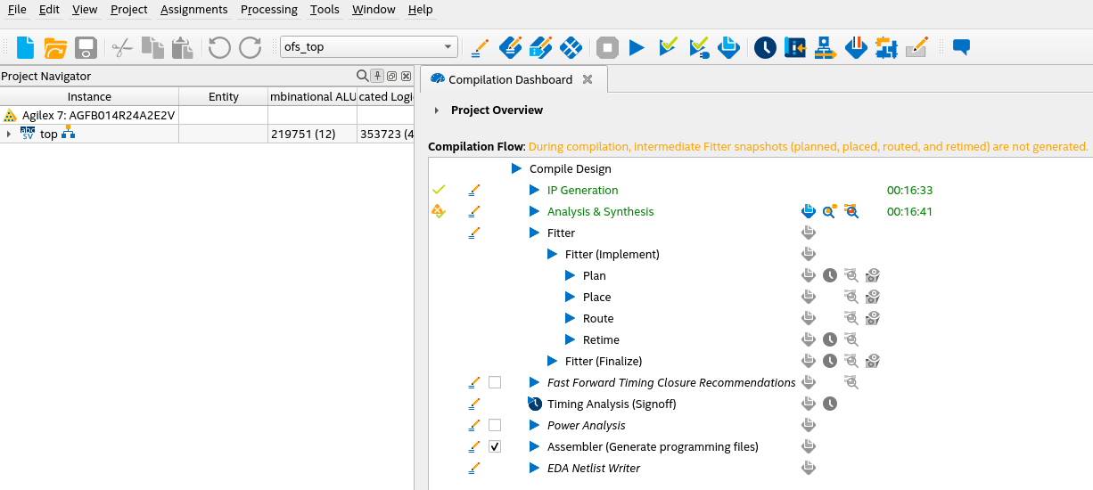
Note: If a full compile has been done in the work directory you are using, you may need to switch from the
ofs_pr_afuview to theofs_topview. -
-
Open Tools -> Signal Tap Logic Analyzer

-
Select the
Defaulttemplate and click Create -
Assign the clock for sampling the Signal Tap instrumented signals of interest. Note that the clock selected should correspond to the signals you want to view for best trace fidelity. Different clocks can be used, however, there maybe issues with trace inaccuracy due to sampling time differences. This example instruments the hello_fim_top module previously intetegrated into the FIM. If unfamiliar with code, it is helpful to use the Quartus Project Navigator to find the block of interest and open the design instance for review.
-
In the Signal Configuration -> Clock box of the Signal Tap Logic Analyzer window, click the "..." button
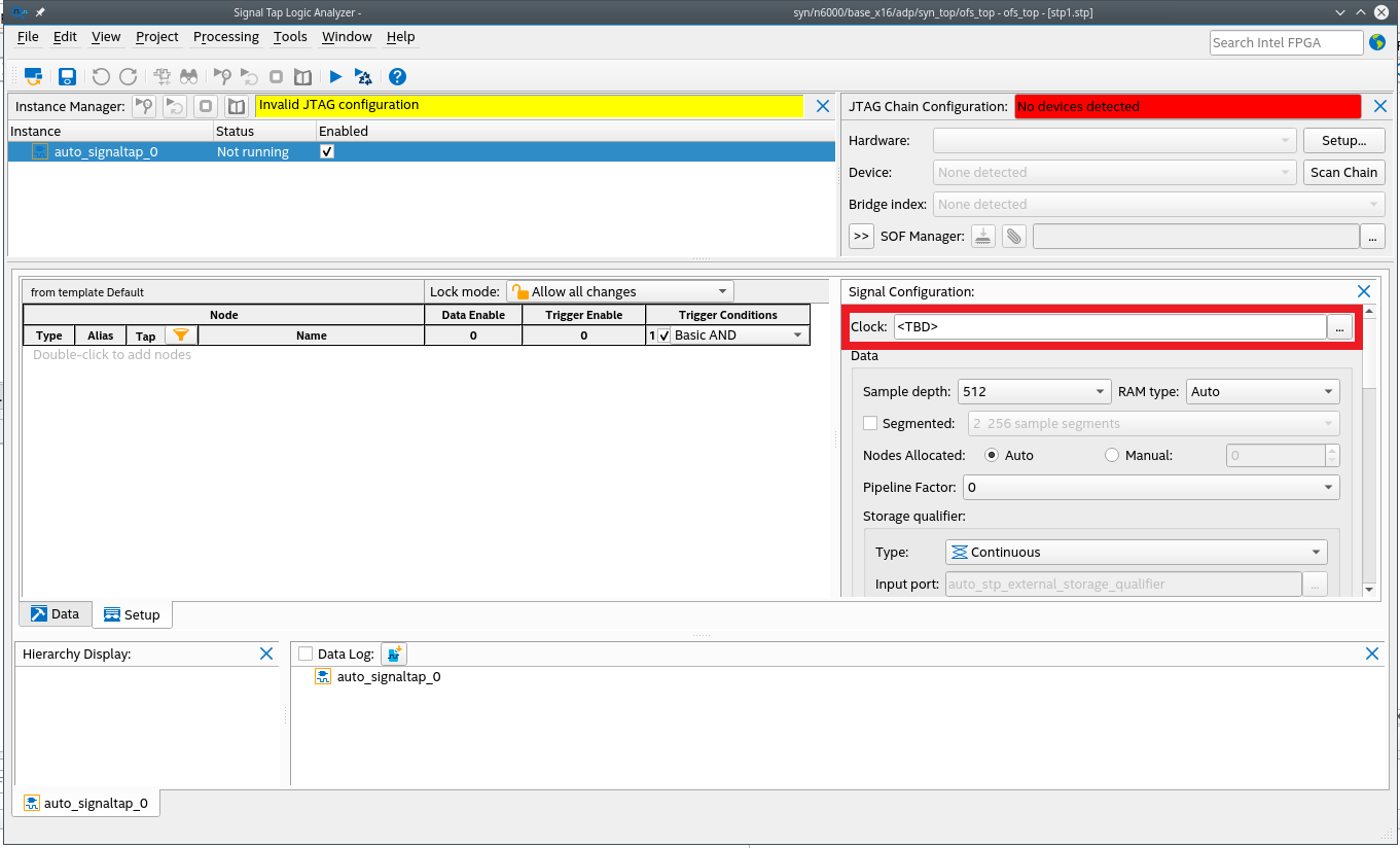
-
In the Node Finder tool that opens, type
clockinto the Named field, and selecthello_fim_top_instin the Look in field, then click Search. Select thehello_fim_top_inst|clksignal from the Matching Nodes box and click the ">" button to move it to the Nodes Found box. Click OK to close the Node Finder dialog.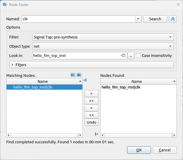
-
-
Update the sample depth and other Signal Tap settings as needed for your debugging criteria.
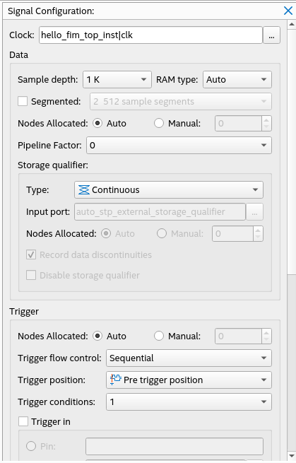
-
In the Signal Tap GUI add the nodes to be instrumented by double-clicking on the "Double-click to add nodes" legend.
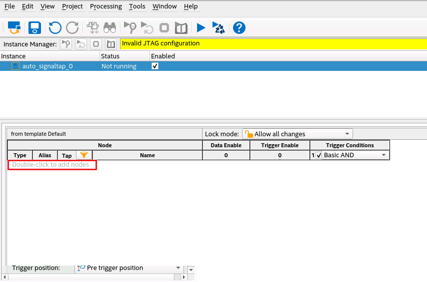
-
This brings up the Node Finder to add the signals to be traced. In this example we will monitor the memory mapped interface to the Hello FIM.
-
In the Named field, enter
csr_lite_if*. In the Look In field, selecthello_fim_top_inst. -
Add the desired nets. In the Object type field select
net. Select the nets that appear in the Matching Nodes box. Click the > button to add them to the Nodes Found box.
-
Add the desired net busses. In the Object type field select
net_bus. Select the busses that appear in the Matching Nodes box. Click the > button to add them to the Nodes Found box.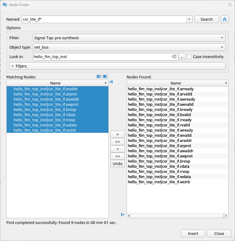
-
Click Insert and close the Node Finder dialog.
-
-
To provide a unique name for your Signal Tap instance, select "auto_signaltap_0", right-click, and select Rename Instance (F2). Provide a descriptive name for your instance, for example,
stp_for_hello_fim.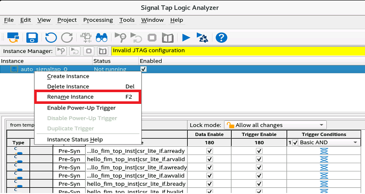
-
Save the newly created Signal Tap file, in the
$OFS_ROOTDIR/work_hello_fim_with_stp/syn/board/n6001/syn_top/directory, and give it the same name as the instance. Ensure that the Add file to current project checkbox is ticked.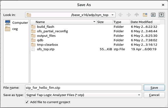
-
In the dialog that pops up, click "Yes" to add the newly created Signal Tap file to the project settings files.
This will automatically add the following lines to
$OFS_ROOTDIR/work_hello_fim_with_stp/syn/board/<board_target>/syn_top/ofs_top.qsf:
-
-
Close all Quartus GUIs.
-
Compile the project with the Signal Tap file added to the project. Use the -k switch to perform the compilation using the files in a specified working directory and not the original ones from the cloned repository.
-
N6001
-
N6000
-
-
Ensure that the compile completes successfully and meets timing.
As an example:
-
Set up a JTAG connection to the n6001 or n6000. Refer to Set up JTAG section for step-by-step instructions.
-
Copy the
ofs_top.sofandstp_for_hello_fim.stpfiles to the machine which is connected to the n6001/n6000 via JTAG. -
From the JTAG connected machine, program the
$OFS_ROOTDIR/work_hello_fim_with_stp/syn/board/<board_target>/syn_top/output_files/ofs_top.sofimage to the n6001 or n6000 FPGA. Refer to the Program the FPGA via JTAG section for step-by-step programming instructions. -
Open the Quartus Signal Tap GUI
-
In the Signal Tap Logic Analyzer window, select File -> Open, and choose the
stp_for_hello_fim.stpfile.
-
In the right pane of the Signal Tap GUI, in the Hardware: selection box select the cable for the n6001/n6000. In the Device: selection box select the Agilex device.

-
If the Agilex Device is not displayed in the Device: list, click the 'Scan Chain' button to re-scan the JTAG device chain.
-
Create the trigger conditions. In this example, we will capture data on a rising edge of the Read Address Valid signal.
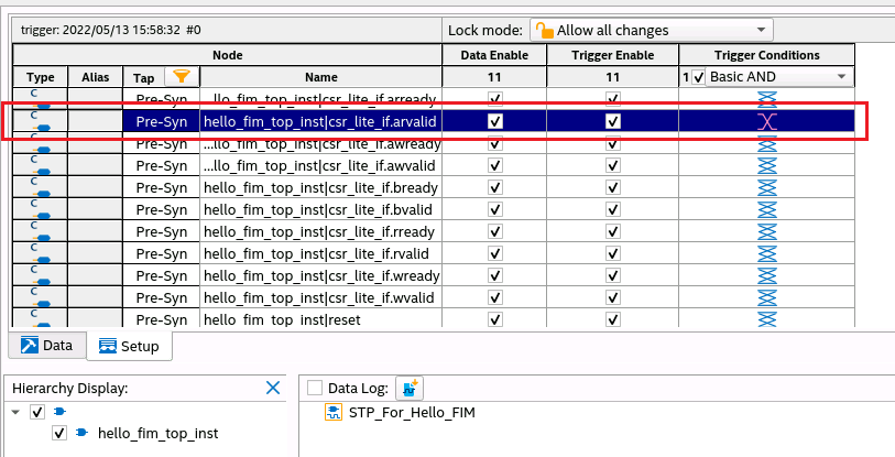
-
Start analysis by selecting the 'stp_for_hello_fim' instance and pressing 'F5' or clicking the Run Analysis icon in the toolbar. You should see a green message indicating the Acquisition is in progress. Then, move to the Data Tab to observe the signals captured.

-
To generate traffic in the csr_lite_if signals of the Hello FIM module, walk the DFH list or peek/poke the Hello FIM registers.
The signals should be captured on the rising edge of
arvalidin this example. Zoom in to get a better view of the signals.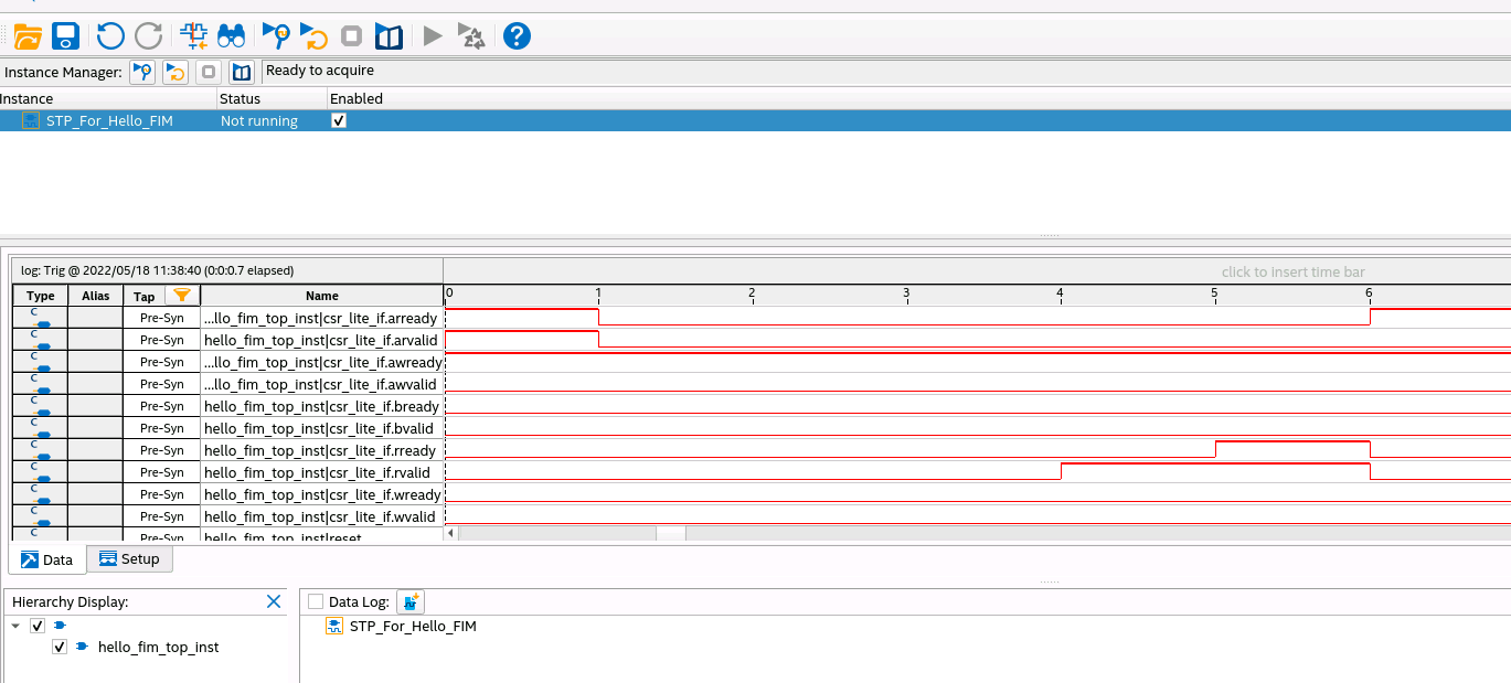
4.2 Preparing FIM for AFU Development
To save area, the default Host Excercisers in the FIM can be replaced by a "he_null" blocks. There are a few things to note:
- "he_null" is a minimal block with registers that responds to PCIe MMIO request. MMIO responses are required to keep PCIe alive (end points enabled in PCIe-SS needs service downstream requests).
- If an exerciser with other I/O connections such as "he_mem" or "he_hssi" is replaced, then then those I/O ports are simply tied off.
- The options supported are
null_he_lb,null_he_hssi,null_he_memandnull_he_mem_tg. Any combination and order can be enabled at the same time. - Finer grain control is provided for you to, for example, turn off only the exercisers in the Static Region in order to save area.
4.2.1 Walkthrough: Compile the FIM in preparation for designing your AFU
Perform the following steps to compile a FIM for where the exercisers are removed and replaced with an he_null module while keeping the PF/VF multiplexor connections.
Pre-requisites:
- This walkthrough requires a development environment. Refer to the Set Up Development Environment Section for instructions on setting up a development environment.
Steps:
-
Clone the FIM repository (or use an existing cloned repository). Refer to the Clone FIM Repository section for step-by-step instructions.
-
Set development environment variables. Refer to the Set Development Environment Variables section for step-by-step instructions.
-
Compile the FIM with the HE_NULL compile options
-
Navigate to the OFS root directory
-
Run the
build_top.shscript with the null host exerciser options.-
N6001
-
N6000
-
-
4.3 Partial Reconfiguration Region
To take advantage of the available resources in the Agilex® 7 FPGA for an AFU design, you can adjust the size of the AFU PR partition. An example reason for the changing the size of PR region is if you add more logic to the FIM region, then you may need to adjust the PR region to fit the additional logic into the static region. Similarly, if you reduce logic in the FIM region, then you can adjust the PR region to provide more logic resources for the AFU.
After the compilation of the FIM, the resources usage broken down by partitions as reported in the following two files
$OFS_ROOTDIR/<WORDK_DIRECTORY>/syn/board/<TARGET_BOARD>/syn_top/output_files/ofs_top.fit.place.rpt
$OFS_ROOTDIR/<WORDK_DIRECTORY>/syn/board/<TARGET_BOARD>/syn_top/output_files/ofs_top.fit.rpt
An example report of the resources usage by partitions defined for the FIM is shown below.
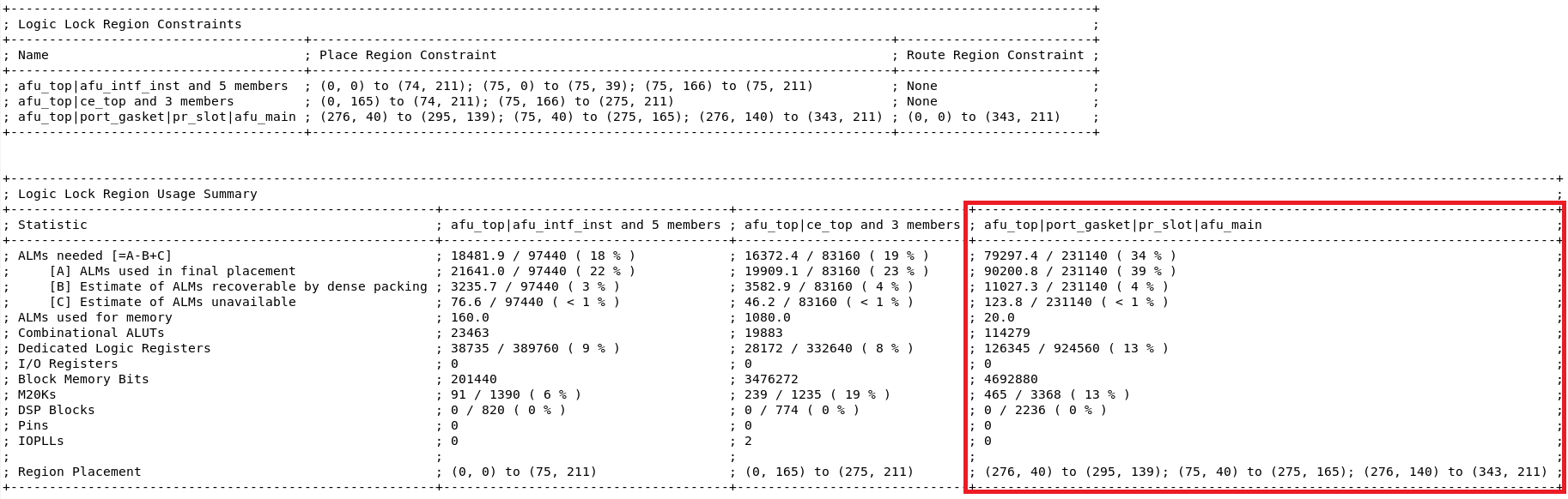
In this case, the default size for the afu_top|port_gasket|pr_slot|afu_main PR partition is large enough to hold the logic of the default AFU, which is mainly occupied by the Host Exercisers. However, larger designs might require additional resources.
4.3.1 Walkthrough: Resize the Partial Reconfiguration Region
Perform the following steps to customize the resources allocated to the AFU in the PR regions:
-
The OFS flow provides the TCL file
$OFS_ROOTDIR/syn/board/<TARGET_BOARD>/setup/pr_assignments.tclwhich defines the PR partition where the AFU is allocated.Example contents of this file for the n6000 are shown as follows:
##################################################### # Main PR Partition -- green_region ##################################################### set_instance_assignment -name PARTITION green_region -to afu_top|pg_afu.port_gasket|pr_slot|afu_main set_instance_assignment -name CORE_ONLY_PLACE_REGION ON -to afu_top|pg_afu.port_gasket|pr_slot|afu_main set_instance_assignment -name RESERVE_PLACE_REGION ON -to afu_top|pg_afu.port_gasket|pr_slot|afu_main set_instance_assignment -name PARTIAL_RECONFIGURATION_PARTITION ON -to afu_top|pg_afu.port_gasket|pr_slot|afu_main set_instance_assignment -name PLACE_REGION "X76 Y30 X300 Y195" -to afu_top|pg_afu.port_gasket|pr_slot|afu_main set_instance_assignment -name ROUTE_REGION "X0 Y0 X344 Y212" -to afu_top|pg_afu.port_gasket|pr_slot|afu_main -
Use Quartus Chip Planner to identify the locations of the resources available within the Agilex® 7 FPGA chip for placement and routing your AFU. You need to identify a pair of coordinates, the origin (X0, Y0) and top right corner (X1, Y1) of the new or existing rectangles to modify as shown in the following image of the n6000 Chip Planner view.

The coordinates of the top right corner of the lock regions are computed indirectly based on the Width and Height, as follows.
-
Make changes to the pr_assignments.tcl based on your findings in Quartus Chip Planner. You can modify the size and location of existing lock regions or add new ones and assign them to the AFU PR partition.
-
Build your FIM and create the PR relocatable build tree using the
build_top.shscript. Refer to the Compile OFS FIM section for step-by-step compilation instructions. -
Analyze the resource utilization report per partition produced after recompiling the FIM.
-
Perform further modification to the PR regions until the results are satisfactory. Make sure timing constraints are met.
For more information on how to optimize the floor plan of your Partial Reconfiguration design refer to the following online documentation.
4.4 PCIe Configuration
The PCIe sub-system IP and PF/VF MUX can be modified either using the OFSS flow or the IP Presets flow. The OFSS flow supports a subset of all available PCIe Sub-system settings, while the IP Preset flow can make any available PCIe Sub-system settings change. With PCIe-SS modifcations related to the PFs and VFs, the PF/VF MUX logic is automatically configured based on the PCIe-SS configuration when using OFSS. The sections below describe each flow.
4.4.1 PF/VF MUX Configuration
The default PF/VF MUX configuration for OFS PCIe Attach FIM for the n6001 can support up to 8 PFs and 2000 VFs distributed accross all PFs.
For reference FIM configurations, you must have at least 1 PF with 1VF, or 2PFs. This is because the PR region cannot be left unconnected. PFs must be consecutive. The PFVF Limitations table describes the supported number of PFs and VFs.
Table: PF/VF Limitations
| Parameter | Value |
|---|---|
| Min # of PFs | 1 (on PF0) |
| Max # of PFs | 8 |
| Min # of VFs | 1 on PF0 (0 if 2PFs present) |
| Max # of VFs | 2000 distributed across all PFs |
New PF or VF instances will automatically have a null_afu module instantiated and connected to the new PF or VF.
4.4.2 PCIe-SS Configuration Registers
The PCIe-SS configuration registers contain the Vendor, Device and Subsystem Vendor ID registers which are used in PCIe add-in cards to uniquely identify the card for assignment to software drivers. OFS has these registers set with Intel values for out of the box usage. If you are using OFS for a PCIe add in card that your company manufactures, then update the PCIe Subsytem Subsystem ID and Vendor ID registers as described below and change OPAE provided software code to properly operate with your company's register values.
The Vendor ID is assigned to your company by the PCI-SIG (Special Interest Group). The PCI-SIG is the only body officially licensed to give out IDs. You must be a member of PCI-SIG to request your own ID. Information about joining PCI-SIG is available here: PCI-SIG. You select the Subsystem Device ID for your PCIe add in card.
4.4.3 PCIe Configuration Using OFSS
The general flow for using OFSS to modify the PCIe Sub-system and PF/VF MUX is as follows:
- Create or modify a PCIe OFSS file with the desired PCIe configuration.
- Call this PCIe OFSS file when running the FIM build script.
The PCIe IP OFSS File Options table lists all of the configuration options supported by the OFSS flow. Any other customizations to the PCIe sub-system must be done with the IP Presets Flow.
Table: PCIe IP OFSS File Options
| Section | Parameter | Options | Default | Description |
|---|---|---|---|---|
[ip] |
type |
pcie |
N/A | Specifies that this OFSS file configures the PCIe-SS |
[settings] |
output_name |
pcie_ss |
N/A | Specifies the output name of the PCIe-SS IP |
preset |
String | N/A | OPTIONAL - Specifies the name of a PCIe-SS IP presets file to use when building the FIM. When used, a presets file will take priority over any other parameters set in this OFSS file. | |
[pf*] |
num_vfs |
Integer | 0 |
Specifies the number of Virtual Functions in the current PF |
bar0_address_width |
Integer | 12 |
||
bar4_address_width |
Integer | 14 |
||
vf_bar0_address_width |
Integer | 12 |
||
ats_cap_enable |
0 | 1 |
0 |
||
vf_ats_cap_enable |
0 | 1 |
0 |
||
prs_ext_cap_enable |
0 | 1 |
0 |
||
pasid_cap_enable |
0 | 1 |
0 |
||
pci_type0_vendor_id |
32'h Value | 0x00008086 |
||
pci_type0_device_id |
32'h Value | 0x0000bcce |
||
revision_id |
32'h Value | 0x00000001 |
||
class_code |
32'h Value | 0x00120000 |
||
subsys_vendor_id |
32'h Value | 0x00008086 |
||
subsys_dev_id |
32'h Value | 0x00001771 |
||
sriov_vf_device_id |
32'h Value | 0x0000bccf |
||
exvf_subsysid |
32'h Value | 0x00001771 |
4.4.3.1 Walkthrough: Modify the PCIe Sub-System and PF/VF MUX Configuration Using OFSS
Perform the following steps to modify the PF/VF MUX configuration.
Pre-requisites:
- This walkthrough requires a development environment. Refer to the Set Up Development Environment Section for instructions on setting up a development environment.
- This walkthrough requires an OFS Agilex PCIe Attach deployment environment. Refer to the Getting Started Guide: OFS for Agilex® 7 PCIe Attach FPGAs (Intel® FPGA SmartNIC N6001-PL/N6000-PL) for instructions on setting up a deployment environment.
Steps:
-
Clone the OFS PCIe Attach FIM repository (or use an existing cloned repository). Refer to the Clone FIM Repository section for step-by-step instructions.
-
Set development environment variables. Refer to the Set Development Environment Variables section for step-by-step instructions.
-
View the default PCIe OFSS file contents. For example, the n6001 default PCIe OFSS configuration is defined in the
$OFS_ROOTDIR/tools/ofss_config/pcie/pcie_host.ofssfile. -
Create a new PCIe OFSS file from the existing
pcie_host.ofssfile -
Configure the new
pcie_pfvf_mod.ofsswith your desired settings. In this example we will add PF5 with 2 VFs. -
Edit the top level OFSS file to use the new PCIe OFSS file
pcie_pf_vf_mod.ofss. In this example, we will edit the n6001 top level OFSS file$OFS_ROOTDIR/tools/ofss_config/n6001.ofss. -
Compile the FIM. In this example we are targeting the n6001 board.
-
Copy the resulting
.binuser 1 image to your deployment environmenment. -
Switch to your deployment environment.
-
Program the
.binimage to the n6001 FPGA. Refer to the Program the FPGA via RSU Section for step-by-step programming instructions. -
Verify the number of VFs on the newly added PF8. In this example, we defined 2 VFs on PF5 in Step 5.
Example output:
-
Verify communication with the newly added PF5. New PF/VF are seamlessly connected to their own CSR stub, which can be read at DFH Offset 0x0. You can bind to the function and perform
opae.io peekcommands to read from the stub CSR. Similarly, performopae.io pokecommands to write into the stub CSRs. Use this mechanism to verify that the new PF/VF Mux configuration allows to write and read back values from the stub CSRs.
The GUID for every new PF/VF CSR stub is the same.
1. Initialize the driver on PF5
```bash
sudo opae.io init -d 98:00.5
```
2. Read the GUID for the PF5 CSR stub.
```bash
sudo opae.io -d 98:00.5 -r 0 peek 0x8
sudo opae.io -d 98:00.5 -r 0 peek 0x10
```

Example output:

```bash
0xaa31f54a3e403501
0x3e7b60a0df2d4850
```
4.4.4 PCIe Sub-System configuration Using IP Presets
The general flow for using IP Presets to modify he PCIe Sub-system is as follows:
- [OPTIONAL] Create a work directory using OFSS files if you wish to use OFSS configuration settings as a starting point.
- Open the PCIe-SS IP and make desired modifications.
- Create an IP Presets file.
- Create an PCIe OFSS file that uses the IP Presets file.
- Build the FIM with the PCIe OFSS file from Step 4.
4.4.4.1 Walkthrough: Modify PCIe Sub-System and PF/VF MUX Configuration Using IP Presets
Perform the following steps to use an IP preset file to configure the PCIe Sub-system and PF/VF MUX. In this example, we will change the Revision ID on PF0. While this modification can be done with the OFSS flow, this walkthrough is intended to show the procedure for making any PCIe configuration change using IP presets. This walkthrough targets the n6001, but similar steps can be applied to the n6000.
Pre-requisites:
- This walkthrough requires a development environment to build the FIM. Refer to the Set Up Development Environment Section for instructions on setting up a development environment.
- This walkthrough requires an OFS Agilex PCIe Attach deployment environment to test the design. Refer to the Getting Started Guide: OFS for Agilex® 7 PCIe Attach FPGAs (Intel® FPGA SmartNIC N6001-PL/N6000-PL) for instructions on setting up a deployment environment.
Steps:
-
Clone the OFS PCIe Attach FIM repository (or use an existing cloned repository). Refer to the Clone FIM Repository section for step-by-step instructions.
-
Set development environment variables. Refer to the Set Development Environment Variables section for step-by-step instructions.
-
[OPTIONAL] Run the
setupstage of the build script using your desired OFSS configration to create a working directory for the target board. In this example we will target the n6001. -
Open the PCIe-SS in the work directory using Quartus Parameter Editor. If you performed Step 3, open the PCIe-SS IP from the work directory; otherwise, open the PCIe-SS IP from the source files.
-
Modify the settings as desired. In this example we are changing the Device ID to
0xbccfand the Revision ID to0x2. In the IP Parameter Editor, scroll down and expand the PCIe Interfaces Ports Settings -> Port 0 -> PCIe0 Device Identification Registers -> PCIe0 PF0 IDs tab and make these changes.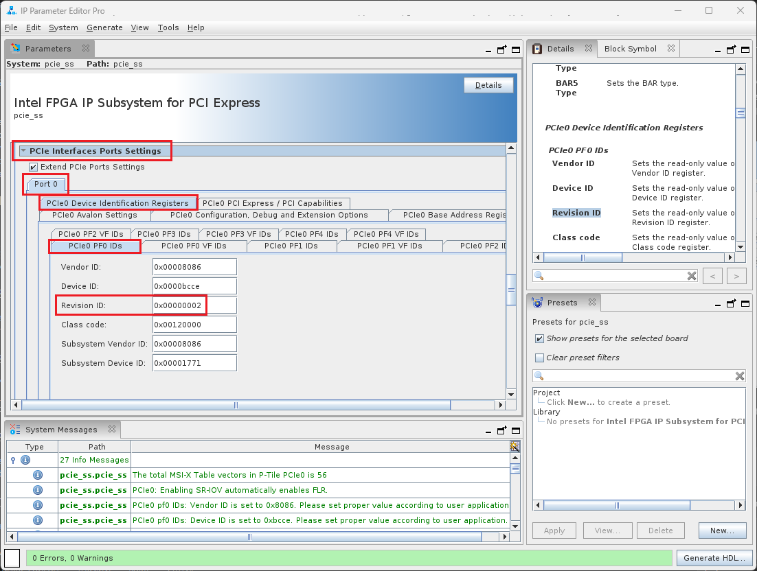
-
Once you are satisfied with your modifcations, create a new IP Preset file.
-
click New... in the Presets window.
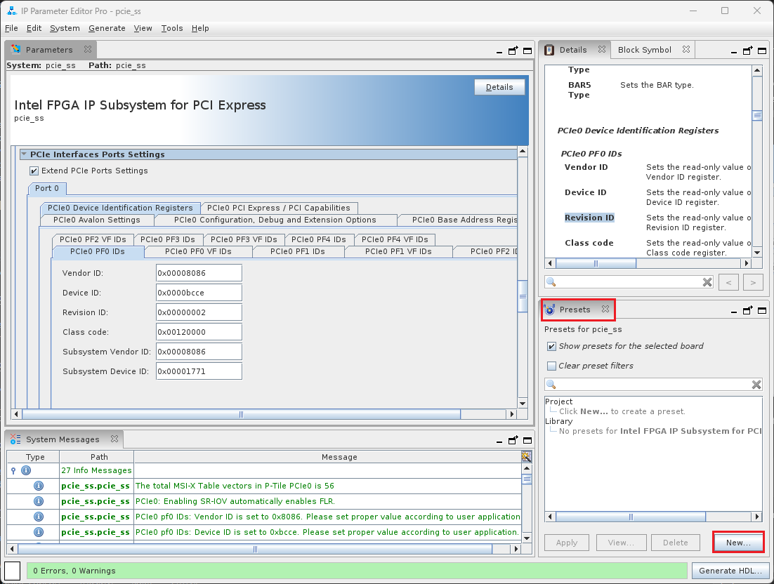
-
In the New Preset window, set a unique Name for the preset; for example,
n6001-rev2.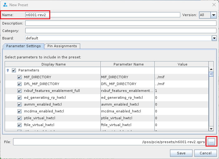
-
Click the ... button to set the save location for the IP Preset file to
$OFS_ROOTDIR/ipss/pcie/presets. Set the File Name to match the name selected in Step 9. Click OK.
-
In the New Preset window, click Save. Click No when prompted to add the file to the IP search path.
-
-
Close IP Parameter Editor without saving or generating HDL.
-
Create a new PCIe OFSS file in the
$OFS_ROOTDIR/tools/ofss_config/pciedirectory. For example:Insert the following into the OFSS file to specify the IP Preset file created in Step 6.
-
Edit the
$OFS_ROOTDIR/tools/ofss_config/n6001.ofssfile to call new OFSS file created in Step 10.[include] "$OFS_ROOTDIR"/tools/ofss_config/n6001_base.ofss "$OFS_ROOTDIR"/tools/ofss_config/pcie/pcie_host_mod_preset.ofss "$OFS_ROOTDIR"/tools/ofss_config/iopll/iopll.ofss "$OFS_ROOTDIR"/tools/ofss_config/memory/memory.ofss -
Compile the design with the modified n6001.ofss file.
-
Copy the resulting
$OFS_ROOTDIR/work_n6001_pcie_mod/syn/board/n6001/syn_top/output_files/ofs_top_hps.sofimage to your deployment environmenment for JTAG programming, or copy abinfile (e.g.ofs_top_page1_unsigned_user1.bin) for RSU programming.Note: OPAE FPGA management commands require recognition of the FPGA PCIe Device ID for control. If there is a problem between OPAE management recognition of FPGA PCIe values, then control of the card will be lost. For this reason, you are strongly encouraged to program the FPGA via JTAG to load the test FPGA image. If there is a problem with the SOF image working with your host software that is updated for the new PCIe settings, then you can load a known good SOF file to recover. Once you sure that both the software and FPGA work properly, you can load the FPGA into FPGA flash using the OPAE command
fpgasupdate. -
Switch to your deployment environment.
-
Program the image to the n6001 FPGA. Refer to the Program the FPGA via JTAG Section for step-by-step JTAG programming instructions, or the Program the FPGA via RSU Section for step-by-step RSU programming instructions.
-
Use
lspcito verify that the PCIe changes have been implemented.Example output:
4.5 Minimal FIM
In a minimal FIM, the exercisers and Ethernet subsystem are removed from the design, and the AFU PR area is expanded to make use of the available area previously used by the removed components. This minimal FIM is useful for HDL applications.
There are two types of provided minimal FIMs:
- 2PF: this minimal FIM has two physical functions, with the APF/BPF on PF0, and the AFU PR region on PF1.

- 1PF/1VF: This minmal FIM has a single physical function, with the APF/BPF on PF0, and the AFU PR region on PF0-VF0.
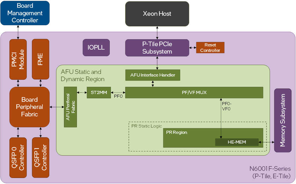
The FIM source repository contains OFSS file that can be used to build the two different types of minimal FIM.
$OFS_ROOTDIR/tools/ofss_config/n6001_2pf.ofss$OFS_ROOTDIR/tools/ofss_config/n6001_1pf_1vf.ofss
4.5.1 Walkthrough: Create a Minimal FIM
Perform the following steps to create a Minimal FIM. A minimal FIM is one that has the host exercisers and ethernet subsystem removed. This frees up resources that can be used.
Pre-requisites:
- This walkthrough requires a development environment. Refer to the Set Up Development Environment Section for instructions on setting up a development environment.
- This walkthrough requires an OFS Agilex PCIe Attach deployment environment. Refer to the Getting Started Guide: OFS for Agilex® 7 PCIe Attach FPGAs (Intel® FPGA SmartNIC N6001-PL/N6000-PL) for instructions on setting up a deployment environment.
Steps:
-
Clone the OFS PCIe Attach FIM repository (or use an existing cloned repository). Refer to the Clone FIM Repository section for step-by-step instructions.
-
Set development environment variables. Refer to the Set Development Environment Variables section for step-by-step instructions.
-
[N6001 ONLY] The OFS FIM repo provides a PR assignments TCL file which optimizes the PR region for the minimal FIM. Copy the minimal PR assignments TCL file into the
pr_assignments.tclfile location for use in the FIM build process.-
Rename the current
pr_assignments.tclfile topr_assignments_base.tclfor future use -
Copy the
pr_assignments_slim.tclfile topr_assignments.tclto be used in the current build
-
-
Compile the FIM with Null HEs compile option, the No HSSI compile option, and the desired configuration OFSS file.
-
For 2PF Minimal FIM
-
For 1PF/1VF Minimal FIM
-
-
Review the
$OFS_ROOTDIR/work_n6001_minimal_fim/syn/board/n6001/syn_top/output_files/ofs_top.fit.rptutilization report to see the utilization statistics for the Minimal fim. Refer to Appendix A: Resource Utilization Tables Table A-4 for the expected utilization for this Minimal FIM. -
Copy the resulting
$OFS_ROOTDIR/work_n6001_minimal_fim/syn/board/n6001/syn_top/output_files/ofs_top.sofimage to your deployment environmenment. -
Switch to your deployment environment, if different than your development environment.
-
Program the
.binimage to the n6001 FPGA. Refer to the Program the FPGA via RSU Section for step-by-step programming instructions. -
Verify the minimal FIM design on the board.
-
For 2PF Minimal FIM:
- Use
opae.io lsto verify that there are two PFs
Example output:
[0000:98:00.1] (0x8086:0xbcce 0x8086:0x1771) Intel Acceleration Development Platform N6001 (Driver: dfl-pci) [0000:98:00.0] (0x8086:0xbcce 0x8086:0x1771) Intel Acceleration Development Platform N6001 (Driver: dfl-pci)-
Use
fpgainfo portto verify the ports.Example output:
//****** PORT ******// Interface : DFL Object Id : 0xEE00000 PCIe s:b:d.f : 0000:98:00.0 Vendor Id : 0x8086 Device Id : 0xBCCE SubVendor Id : 0x8086 SubDevice Id : 0x1771 Socket Id : 0x00 //****** PORT ******// Interface : UIO Object Id : 0xED00000 PCIe s:b:d.f : 0000:98:00.0 Vendor Id : 0x8086 Device Id : 0xBCCE SubVendor Id : 0x8086 SubDevice Id : 0x1771 Socket Id : 0x01 Accelerator GUID : 00000000-0000-0000-0000-000000000000 -
Bind the VFIO driver on PF1.
Example output:
-
Use
fpgainfo portto verify the ports. There should now be a port entry for PF1. The Accelerator GUID for PF1 should be as shown below, which is the GUID for the HE-MEM.//****** PORT ******// Interface : DFL Object Id : 0xEE00000 PCIe s:b:d.f : 0000:98:00.0 Vendor Id : 0x8086 Device Id : 0xBCCE SubVendor Id : 0x8086 SubDevice Id : 0x1771 Socket Id : 0x00 //****** PORT ******// Interface : VFIO Object Id : 0x2098000000000000 PCIe s:b:d.f : 0000:98:00.1 Vendor Id : 0x8086 Device Id : 0xBCCE SubVendor Id : 0x8086 SubDevice Id : 0x1771 Socket Id : 0x01 Accelerator GUID : 8568ab4e-6ba5-4616-bb65-2a578330a8eb //****** PORT ******// Interface : UIO Object Id : 0xED00000 PCIe s:b:d.f : 0000:98:00.0 Vendor Id : 0x8086 Device Id : 0xBCCE SubVendor Id : 0x8086 SubDevice Id : 0x1771 Socket Id : 0x01 Accelerator GUID : 00000000-0000-0000-0000-000000000000
- Use
-
For 1PF/1VF Minimal FIM:
- Use
opae.io lsto verify that there is one PF.
Example output:
[0000:98:00.0] (0x8086:0xbcce 0x8086:0x1771) Intel Acceleration Development Platform N6001 (Driver: dfl-pci)-
Use
lspcito verify that there is 1 VF on PF0.Example output:
-
Use
fpgainfo portto verify the ports.Example output:
//****** PORT ******// Interface : DFL Object Id : 0xEE00000 PCIe s:b:d.f : 0000:98:00.0 Vendor Id : 0x8086 Device Id : 0xBCCE SubVendor Id : 0x8086 SubDevice Id : 0x1771 Socket Id : 0x00 //****** PORT ******// Interface : UIO Object Id : 0xED00000 PCIe s:b:d.f : 0000:98:00.0 Vendor Id : 0x8086 Device Id : 0xBCCE SubVendor Id : 0x8086 SubDevice Id : 0x1771 Socket Id : 0x01 Accelerator GUID : 00000000-0000-0000-0000-000000000000 -
Initialize one virtual function
-
Use
opae.io lsto verify the VF has been initialized.Example output:
-
Bind the VFIO driver on VF0
-
Use
fpgainfo portto verify the ports. There should now be a port entry for VF0. The Accelerator GUID for VF0 should be as shown below, which is the GUID for the HE-MEM.Example output:
//****** PORT ******//
Interface                        : DFL
Object Id                        : 0xEE00000
PCIe s:b:d.f                     : 0000:98:00.0
Vendor Id                        : 0x8086
Device Id                        : 0xBCCE
SubVendor Id                     : 0x8086
SubDevice Id                     : 0x1771
Socket Id                        : 0x00
//****** PORT ******//
Interface                        : VFIO
Object Id                        : 0x2098000000000000
PCIe s:b:d.f                     : 0000:98:00.1
Vendor Id                        : 0x8086
Device Id                        : 0xBCCF
SubVendor Id                     : 0x8086
SubDevice Id                     : 0x1771
Socket Id                        : 0x01
Accelerator GUID                 : 8568ab4e-6ba5-4616-bb65-2a578330a8eb
//****** PORT ******//
Interface                        : UIO
Object Id                        : 0xED00000
PCIe s:b:d.f                     : 0000:98:00.0
Vendor Id                        : 0x8086
Device Id                        : 0xBCCE
SubVendor Id                     : 0x8086
SubDevice Id                     : 0x1771
Socket Id                        : 0x01
Accelerator GUID                 : 00000000-0000-0000-0000-000000000000
- Use
-
4.6 Migrate to a Different Agilex Device Number
The following instructions enable a user to change the device part number of the Intel® FPGA SmartNIC N6001-PL. Please be aware that this release works with Agilex® 7 FPGA devices that have P tile for PCIe and E tile for Ethernet. Other tiles will take further work.
You may wish to change the device part number for the following reasons
- Migrate to same device package but with a different density
- Migrate to a different package and with a different or same density
The default device for the Intel® FPGA SmartNIC N6001-PL is AGFB014R24A2E2V
4.6.1 Walkthrough: Migrate to a Different Agilex Device Number
Perform the following steps to migrate your design to target a different Agilex device using the OFSS build flow. In this example we will change the device from the default AGFB014R24A2E2V to a new device AGFB022R25A2E2V. This walkthrough will target the n6001, but similar steps can be used for the n6000.
Pre-requisites:
- This walkthrough requires a development environment. Refer to the Set Up Development Environment Section for instructions on setting up a development environment.
Steps:
-
Clone the OFS PCIe Attach FIM repository (or use an existing cloned repository). Refer to the Clone FIM Repository section for step-by-step instructions.
-
Set development environment variables. Refer to the Set Development Environment Variables section for step-by-step instructions.
-
Modify the
partfield in the$OFS_ROOTDIR/tools/ofss_config/n6001_base.ofssfile to useAGFB022R25A2E2V. This is only necessary if you are using the OFSS flow. -
Modify the
DEVICEfield in the$OFS_ROOTDIR/syn/board/n6001/syn_top/ofs_top.qsffile. -
Modify the
DEVICEfield in the$OFS_ROOTDIR/syn/board/n6001/syn_top/ofs_pr_afu.qsffile. -
Modify the
DEVICEfield in te$OFS_ROOTDIR/ipss/pmci/pmci_ss.qsffile. -
If you are changing to a device with a different package, you must change the pin assignments in the location files. If you would like Quartus to attempt to pin out the design automatically, you may remove all pin assignments instead. Typically you will be required to set certain pins manually in order to guide Quartus for a successful compile (e.g. transceiver reference clocks). In this example we will start by commenting out all of the pin constraints in the following files and attempt to let Quartus pin out the design as much as possibe:
$OFS_ROOTDIR/syn/board/n6001/setup/emif_loc.tcl
$OFS_ROOTDIR/syn/board/n6001/setup/hps_loc.tcl
$OFS_ROOTDIR/syn/board/n6001/setup/pmci_loc.tcl
$OFS_ROOTDIR/syn/board/n6001/setup/top_loc.tcl
For example:
-
Identify the pins you wish to assign prior to compiling. In this example, we will re-pin some of the reference clocks to help guide the fitter. Refer to the Pin-Out Files for Altera FPGAs for the pin list of your device. In this example, the Migration Re-Pin Mapping table below shows the pins we will re-pin in the constraints files.
Table: Migration Re-Pin Mapping
Pin Name FIM Signal Name AGF 014 R24A Pin # AGF 022 R25A Pin # REFCLK_GXER9A_CH0p cr3_cpri_reflclk_clk[0]PIN_AT13 PIN_CE18 REFCLK_GXER9A_CH0n "cr3_cpri_reflclk_clk[0](n)"PIN_AP13 PIN_CA18 REFCLK_GXER9A_CH1p cr3_cpri_refclk_clk[1]PIN_AR14 PIN_CC19 REFCLK_GXER9A_CH1n "cr3_cpri_refclk_clk[1](n)"PIN_AN14 PIN_BW19 REFCLK_GXER9A_CH2p cr3_cpri_refclk_clk[2]PIN_AJ12 PIN_BL17 REFCLK_GXER9A_CH2n "cr3_cpri_refclk_clk[2](n)"PIN_AH11 PIN_BJ15 REFCLK_GXER9A_CH3p qsfp_ref_clkPIN_AK13 PIN_BN18 REFCLK_GXER9A_CH3n "qsfp_ref_clk(n)"PIN_AH13 PIN_BJ18 REFCLK_GXER9A_CH4p cr3_cpri_reflclk_clk_184_32mPIN_AJ14 PIN_BL19 REFCLK_GXER9A_CH4n "cr3_cpri_reflclk_clk_184_32m(n)"PIN_AL14 PIN_BR19 REFCLK_GXER9A_CH5p cr3_cpri_reflclk_clk_153_6mPIN_AR16 PIN_CC21 REFCLK_GXER9A_CH5n "cr3_cpri_reflclk_clk_153_6m(n)"PIN_AN16 PIN_BW21 REFCLK_GXPL10A_CH0n "PCIE_REFCLK0(n)"PIN_AH49 PIN_DD56 REFCLK_GXPL10A_CH0p PCIE_REFCLK0PIN_AJ48 PIN_DF57 REFCLK_GXPL10A_CH2n "PCIE_REFCLK1(n)"PIN_AD49 PIN_CT56 REFCLK_GXPL10A_CH2p PCIE_REFCLK1PIN_AE48 PIN_CV57 -
Re-pin the reference clocks defined in
$OFS_ROOTDIR/syn/board/n6001/setup/top_loc.tclset_location_assignment PIN_BN18 -to qsfp_ref_clk set_location_assignment PIN_BJ18 -to "qsfp_ref_clk(n)" set_location_assignment PIN_CC19 -to cr3_cpri_refclk_clk[1] set_location_assignment PIN_BW19 -to "cr3_cpri_refclk_clk[1](n)" set_location_assignment PIN_BL17 -to cr3_cpri_refclk_clk[2] set_location_assignment PIN_BJ15 -to "cr3_cpri_refclk_clk[2](n)" set_location_assignment PIN_CE18 -to cr3_cpri_reflclk_clk[0] set_location_assignment PIN_CA18 -to "cr3_cpri_reflclk_clk[0](n)" set_location_assignment PIN_BL19 -to cr3_cpri_reflclk_clk_184_32m set_location_assignment PIN_BR19 -to "cr3_cpri_reflclk_clk_184_32m(n)" set_location_assignment PIN_CC21 -to cr3_cpri_reflclk_clk_153_6m set_location_assignment PIN_BW21 -to "cr3_cpri_reflclk_clk_153_6m(n)" set_location_assignment PIN_DD56 -to "PCIE_REFCLK0(n)" set_location_assignment PIN_DF57 -to PCIE_REFCLK0 set_location_assignment PIN_CT56 -to "PCIE_REFCLK1(n)" set_location_assignment PIN_CV57 -to PCIE_REFCLK1 -
Un-comment the instance assignemnts for the transceiver reference clocks defined in
$OFS_ROOTDIR/syn/board/n6001/setup/top_loc.tcl.set_instance_assignment -name IO_STANDARD "DIFFERENTIAL LVPECL" -to qsfp_ref_clk set_instance_assignment -name HSSI_PARAMETER "refclk_divider_enable_termination=enable_term" -to qsfp_ref_clk set_instance_assignment -name HSSI_PARAMETER "refclk_divider_enable_3p3v=disable_3p3v_tol" -to qsfp_ref_clk set_instance_assignment -name HSSI_PARAMETER "refclk_divider_disable_hysteresis=enable_hyst" -to qsfp_ref_clk set_instance_assignment -name HSSI_PARAMETER "refclk_divider_input_freq=156250000" -to qsfp_ref_clk set_instance_assignment -name HSSI_PARAMETER "refclk_divider_powerdown_mode=false" -to qsfp_ref_clk set_instance_assignment -name HSSI_PARAMETER "refclk_divider_use_as_bti_clock=TRUE" -to qsfp_ref_clk set_instance_assignment -name IO_STANDARD "DIFFERENTIAL LVPECL" -to cr3_cpri_refclk_clk[1] set_instance_assignment -name HSSI_PARAMETER "refclk_divider_enable_termination=enable_term" -to cr3_cpri_refclk_clk[1] set_instance_assignment -name HSSI_PARAMETER "refclk_divider_enable_3p3v=disable_3p3v_tol" -to cr3_cpri_refclk_clk[1] set_instance_assignment -name HSSI_PARAMETER "refclk_divider_disable_hysteresis=enable_hyst" -to cr3_cpri_refclk_clk[1] set_instance_assignment -name HSSI_PARAMETER "refclk_divider_input_freq=184320000" -to cr3_cpri_refclk_clk[1] set_instance_assignment -name HSSI_PARAMETER "refclk_divider_powerdown_mode=false" -to cr3_cpri_refclk_clk[1] set_instance_assignment -name HSSI_PARAMETER "refclk_divider_use_as_bti_clock=FALSE" -to cr3_cpri_refclk_clk[1] set_instance_assignment -name IO_STANDARD "DIFFERENTIAL LVPECL" -to cr3_cpri_refclk_clk[2] set_instance_assignment -name HSSI_PARAMETER "refclk_divider_enable_termination=enable_term" -to cr3_cpri_refclk_clk[2] set_instance_assignment -name HSSI_PARAMETER "refclk_divider_enable_3p3v=disable_3p3v_tol" -to cr3_cpri_refclk_clk[2] set_instance_assignment -name HSSI_PARAMETER "refclk_divider_disable_hysteresis=enable_hyst" -to cr3_cpri_refclk_clk[2] set_instance_assignment -name HSSI_PARAMETER "refclk_divider_input_freq=153600000" -to cr3_cpri_refclk_clk[2] set_instance_assignment -name HSSI_PARAMETER "refclk_divider_powerdown_mode=false" -to cr3_cpri_refclk_clk[2] set_instance_assignment -name HSSI_PARAMETER "refclk_divider_use_as_bti_clock=FALSE" -to cr3_cpri_refclk_clk[2] set_instance_assignment -name IO_STANDARD "DIFFERENTIAL LVPECL" -to cr3_cpri_reflclk_clk[0] set_instance_assignment -name HSSI_PARAMETER "refclk_divider_enable_termination=enable_term" -to cr3_cpri_reflclk_clk[0] set_instance_assignment -name HSSI_PARAMETER "refclk_divider_enable_3p3v=disable_3p3v_tol" -to cr3_cpri_reflclk_clk[0] set_instance_assignment -name HSSI_PARAMETER "refclk_divider_disable_hysteresis=enable_hyst" -to cr3_cpri_reflclk_clk[0] set_instance_assignment -name HSSI_PARAMETER "refclk_divider_input_freq=245760000" -to cr3_cpri_reflclk_clk[0] set_instance_assignment -name HSSI_PARAMETER "refclk_divider_powerdown_mode=false" -to cr3_cpri_reflclk_clk[0] set_instance_assignment -name HSSI_PARAMETER "refclk_divider_use_as_bti_clock=FALSE" -to cr3_cpri_reflclk_clk[0] set_instance_assignment -name IO_STANDARD "DIFFERENTIAL LVPECL" -to cr3_cpri_reflclk_clk_184_32m set_instance_assignment -name HSSI_PARAMETER "refclk_divider_enable_termination=enable_term" -to cr3_cpri_reflclk_clk_184_32m set_instance_assignment -name HSSI_PARAMETER "refclk_divider_enable_3p3v=enable_3p3v_tol" -to cr3_cpri_reflclk_clk_184_32m set_instance_assignment -name HSSI_PARAMETER "refclk_divider_disable_hysteresis=enable_hyst" -to cr3_cpri_reflclk_clk_184_32m set_instance_assignment -name HSSI_PARAMETER "refclk_divider_input_freq=184320000" -to cr3_cpri_reflclk_clk_184_32m set_instance_assignment -name HSSI_PARAMETER "refclk_divider_powerdown_mode=false" -to cr3_cpri_reflclk_clk_184_32m set_instance_assignment -name HSSI_PARAMETER "refclk_divider_use_as_bti_clock=FALSE" -to cr3_cpri_reflclk_clk_184_32m set_instance_assignment -name IO_STANDARD "DIFFERENTIAL LVPECL" -to cr3_cpri_reflclk_clk_153_6m set_instance_assignment -name HSSI_PARAMETER "refclk_divider_enable_termination=enable_term" -to cr3_cpri_reflclk_clk_153_6m set_instance_assignment -name HSSI_PARAMETER "refclk_divider_enable_3p3v=enable_3p3v_tol" -to cr3_cpri_reflclk_clk_153_6m set_instance_assignment -name HSSI_PARAMETER "refclk_divider_disable_hysteresis=enable_hyst" -to cr3_cpri_reflclk_clk_153_6m set_instance_assignment -name HSSI_PARAMETER "refclk_divider_input_freq=153600000" -to cr3_cpri_reflclk_clk_153_6m set_instance_assignment -name HSSI_PARAMETER "refclk_divider_powerdown_mode=false" -to cr3_cpri_reflclk_clk_153_6m set_instance_assignment -name HSSI_PARAMETER "refclk_divider_use_as_bti_clock=FALSE" -to cr3_cpri_reflclk_clk_153_6m -
Compile a flat design. It is recommended to compile a flat design first before incorporating a PR region in the design. This reduces design complexity while you determine the correct pinout for your design.
-
The compile should succeed. If the compile fails with errors relating to the pinout, review the error messages and modify the pinout.
-
After a successful compile, to preserve pin assignemnts you must hard code the new pin asigments back to the constraints files.
4.7 Modify the Memory Sub-System
OFS allows modifications on the Memory Sub-System in the FIM. This section provides an example walkthrough for modifiying the Memory-SS.
4.7.1 Walkthrough: Modify the Memory Sub-System Using IP Presets With OFSS
This walkthrough will go through the flow of modifying the Memory-SS in the OFS FIM. In this example, we will enable ECC on memory channels 0-3. Note that routes for the ECC pins on Channels 0 and 1 are not physiclly present on standard n6001/n6000 board hardware; the purpose of this walkthrough is only to show an example of how to make modifications to the IP. This walkthrough targets the n6001 board, but similar steps can be used for the n6000.
Pre-requisites:
- This walkthrough requires a development environment. Refer to the Set Up Development Environment Section for instructions on setting up a development environment.
Steps:
-
Clone the OFS PCIe Attach FIM repository (or use an existing cloned repository). Refer to the Clone FIM Repository section for step-by-step instructions.
-
Set development environment variables. Refer to the Set Development Environment Variables section for step-by-step instructions.
-
Open the Memory Subsystem
mem_ss.ipin IP Parameter Editor -
The Memory Subsystem IP will open in IP Parameter Editor. Click Dive Into Packaged Subsystem.
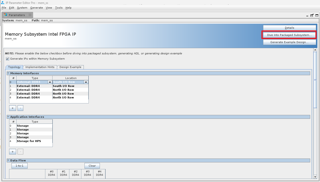
-
The Platform Designer mem_ss view opens. All of the EMIFs are shown in the Filter window.

-
Click each EMIF 0 through 3 and perform the following actions.
-
In the Parameters window, click the Memory tab and change the DQ width to
40.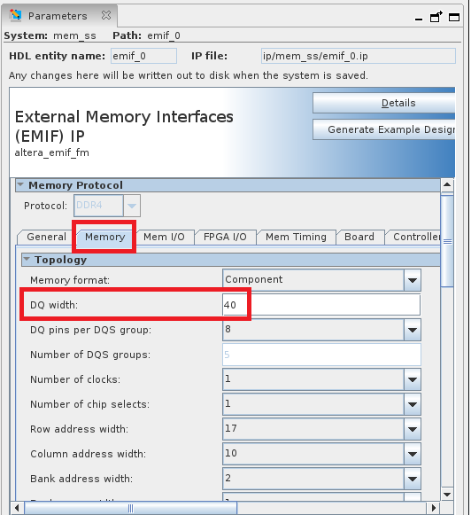
-
In the Parameters window, click the Controller tab.

-
Scroll down and check the box for
Enable Error Detection and Correction Logic with ECC.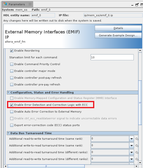
-
-
Once Step 6 has been done for each EMIF 0-3, click File -> Save. Close the Platform Designer window.
-
In the IP Parameter Editor Presets window, click New to create an IP Presets file.
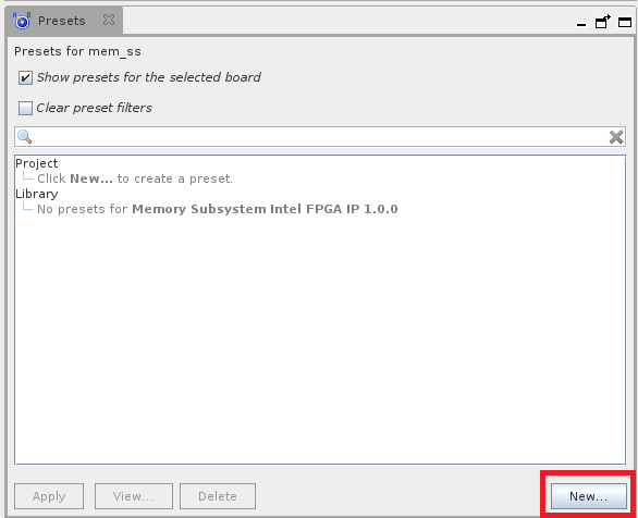
-
In the New Preset window, set the Name for the preset. In this case we will name it
n6001-ecc.
-
Click the ... button to select the location for the Preset file.
-
In the Save As window, change the save location to
$OFS_ROOTDIR/ipss/mem/qip/presetsand change the File Name ton6001-ecc.qprs. Click OK.
-
Click Save in the New Preset window. Click No when prompted to add the file to the IP search path.
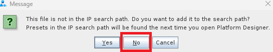
-
Close the IP Parameter Editor. You do not need to generate or save the IP.
-
Edit the
$OFS_ROOTDIR/syn/board/n6001/setup/emif_loc.tclfile to add pin assignments for the new signals supporting ECC on Channels 0-3. Note that routes for the ECC pins on Channels 0 and 1 are not physiclly present on a standard n6001 board.# CH0 DQS4 (ECC) set_location_assignment PIN_CG48 -to ddr4_mem[0].dbi_n[4] set_location_assignment PIN_CF47 -to ddr4_mem[0].dqs_n[4] set_location_assignment PIN_CH47 -to ddr4_mem[0].dqs[4] set_location_assignment PIN_CE50 -to ddr4_mem[0].dq[32] set_location_assignment PIN_CG50 -to ddr4_mem[0].dq[33] set_location_assignment PIN_CF49 -to ddr4_mem[0].dq[34] set_location_assignment PIN_CH49 -to ddr4_mem[0].dq[35] set_location_assignment PIN_CE46 -to ddr4_mem[0].dq[36] set_location_assignment PIN_CG46 -to ddr4_mem[0].dq[37] set_location_assignment PIN_CF45 -to ddr4_mem[0].dq[38] set_location_assignment PIN_CH45 -to ddr4_mem[0].dq[39] # CH1 DQS4 (ECC) set_location_assignment PIN_DC34 -to ddr4_mem[1].dbi_n[4] set_location_assignment PIN_CY33 -to ddr4_mem[1].dqs_n[4] set_location_assignment PIN_DB33 -to ddr4_mem[1].dqs[4] set_location_assignment PIN_DA36 -to ddr4_mem[1].dq[32] set_location_assignment PIN_DC36 -to ddr4_mem[1].dq[33] set_location_assignment PIN_CY35 -to ddr4_mem[1].dq[34] set_location_assignment PIN_DB35 -to ddr4_mem[1].dq[35] set_location_assignment PIN_DA32 -to ddr4_mem[1].dq[36] set_location_assignment PIN_DC32 -to ddr4_mem[1].dq[37] set_location_assignment PIN_CY31 -to ddr4_mem[1].dq[38] set_location_assignment PIN_DB31 -to ddr4_mem[1].dq[39] # CH2 DQS4 (ECC) set_location_assignment PIN_G36 -to ddr4_mem[2].dbi_n[4] set_location_assignment PIN_H35 -to ddr4_mem[2].dqs_n[4] set_location_assignment PIN_F35 -to ddr4_mem[2].dqs[4] set_location_assignment PIN_G38 -to ddr4_mem[2].dq[32] set_location_assignment PIN_J38 -to ddr4_mem[2].dq[33] set_location_assignment PIN_H33 -to ddr4_mem[2].dq[34] set_location_assignment PIN_J34 -to ddr4_mem[2].dq[35] set_location_assignment PIN_F33 -to ddr4_mem[2].dq[36] set_location_assignment PIN_H37 -to ddr4_mem[2].dq[37] set_location_assignment PIN_F37 -to ddr4_mem[2].dq[38] set_location_assignment PIN_G34 -to ddr4_mem[2].dq[39] # CH3 DQS4 (ECC) set_location_assignment PIN_L50 -to ddr4_mem[3].dbi_n[4] set_location_assignment PIN_P49 -to ddr4_mem[3].dqs_n[4] set_location_assignment PIN_M49 -to ddr4_mem[3].dqs[4] set_location_assignment PIN_M51 -to ddr4_mem[3].dq[32] set_location_assignment PIN_N48 -to ddr4_mem[3].dq[33] set_location_assignment PIN_M47 -to ddr4_mem[3].dq[34] set_location_assignment PIN_L48 -to ddr4_mem[3].dq[35] set_location_assignment PIN_P47 -to ddr4_mem[3].dq[36] set_location_assignment PIN_P51 -to ddr4_mem[3].dq[37] set_location_assignment PIN_N52 -to ddr4_mem[3].dq[38] set_location_assignment PIN_L52 -to ddr4_mem[3].dq[39] -
Edit the
$OFS_ROOTDIR/tools/ofss_config/memory/memory.ofssfile to use then6001-eccpreset that was generated previously. -
Compile the design with the
n6001.ofssfile, which will use the modifiedmemory.ofssfile.
4.7.2 Walkthrough: Add or remove the Memory Sub-System
The Memory Sub-System can be added or removed to the FIM design using the INCLUDE_DDR4 macro defined in the ofs_top.qsf file. The Memory-SS is enabled by default in the n6001, and is disabled by default in the n6000.
Pre-requisites:
- This walkthrough requires a development environment. Refer to the Set Up Development Environment Section for instructions on setting up a development environment.
Steps:
-
Clone the OFS PCIe Attach FIM repository (or use an existing cloned repository). Refer to the Clone FIM Repository section for step-by-step instructions.
-
Set development environment variables. Refer to the Set Development Environment Variables section for step-by-step instructions.
-
Edit the
ofs_top.qsffile to either enable or disable theINCLUDE_DDR4macro. Comment out this macro assignemnt if you wish to remove the Memory-SS.Note: The default Memory-SS has connections to the HPS. When enabling the Memory-SS, you must either ensure that the
INCLUDE_HPSandINCLUDE_UARTmacros are also enabled, or you must remove the connections from the Memory-SS to the HPS. Refer to the Remove the HPS section for step-by-step instructions on removing the HPS from the design. -
Compile the design. Refer to the Compile OFS FIM section for step-by-step instructions.
4.8 Modify the Ethernet Sub-System
This section describes the flows for modifying the Ethernet Sub-System. There are three flows you may use to make modifications.
- Modify the Ethernet Sub-System with OFSS supported changes only. These modifications are supported natively by the build script, and are made at run-time of the build script. This flow is useful for users who only need to leverage natively supported HSSI OFSS settings.
- Modify the Ethernet Sub-System with OFSS supported changes, then make additional custom modifications not covered by OFSS. These modifications will be captured in a presets file which can be used in future compiles. This flow is useful for users who whish to leverage pre-made HSSI OFSS settings, but make additional modifications not natively supported by HSSI OFSS.
- Modify the Ethernet Sub-System without HSSI OFSS. These modification will be made directly in the source files.
4.8.1 Walkthrough: Modify the Ethernet Sub-System Channels With Pre-Made HSSI OFSS
This walkthrough describes how to use OFSS to configure the Ethernet-SS. Refer to section HSSI IP OFSS File for detailed information about modifications supported by Ethernet-SS OFSS files. This walkthrough is useful for users who only need to leverage the pre-made, natively supported HSSI OFSS settings.
Pre-Requisites:
- This walkthrough requires a development environment. Refer to the Set Up Development Environment Section for instructions on setting up a development environment.
Steps:
-
Clone the OFS PCIe Attach FIM repository (or use an existing cloned repository). Refer to the Clone FIM Repository section for step-by-step instructions.
-
Set development environment variables. Refer to the Set Development Environment Variables section for step-by-step instructions.
-
Edit the
$OFS_ROTDIR/tools/ofss_config/<TARGET_BOARD>.ofssfile to use the desired Ethernet-SS OFSS configuration. The pre-provided OFSS configurations are as follows:-
N6001
-
To select the 2x4x25GbE configuration, include the following line
-
To select the 2x4x10GbE configuration, include the following line
-
To select the 2x1x100GbE configuration, include the following line
-
-
N6000
-
To select the 4x1x100GbE configuration, include the following line
-
-
-
Compile the FIM using the target board OFSS file.
-
N6001
-
N6000
-
-
The resulting FIM will contain the Ethernet-SS configuration specified in Step 3. The Ethernet-SS IP in the resulting work directory shows the parameter settings that are used.
4.8.2 Walkthrough: Add Channels to the Ethernet Sub-System Channels With Custom HSSI OFSS
This walkthrough describes how to create an use a custom OFSS file to add channels to the Ethernet-SS and compile a design with a 3x4x10GbE Ethernet-SS configuration. This walkthrough is useful for users who wish to leverage the natively supported HSSI OFSS settings.
Note: The n6000 uses 16 channels in the HSSI-SS by default: 8 to the QSFPs, and 8 to the E810 device. Thus, this walkthrough applies only to the n6001.
Pre-Requisites:
- This walkthrough requires a development environment. Refer to the Set Up Development Environment Section for instructions on setting up a development environment.
Steps:
-
Clone the OFS PCIe Attach FIM repository (or use an existing cloned repository). Refer to the Clone FIM Repository section for step-by-step instructions.
-
Set development environment variables. Refer to the Set Development Environment Variables section for step-by-step instructions.
-
Create a new HSSI OFSS file
$OFS_ROOTDIR/tools/ofss_config/hssi/hssi_12x10.ofsswith the following contents. -
Edit the
$OFS_ROOTDIR/tools/ofss_config/n6001.ofssfile to use the new HSSI OFSS file generated in Step 3. -
Identify the which channels will be added. You may use the E-Tile Channel Placement Tool to aid in your design. In this example we will add the 4 new 10GbE channels to Channels 8-11.

-
Based on your channel selection, identify which pins will be used. Refer to the Pin-Out Files for Altera FPGAs determine the required pins for your device. In this example we are targeting the AGFB014R24A2E2V device. Set the pin assignments in the
$OFS_ROOTDIR/syn/board/n6001/setup/top_loc.tclfile.set_location_assignment PIN_AV7 -to qsfp_serial[2].rx_p[0] set_location_assignment PIN_AW10 -to qsfp_serial[2].rx_p[1] set_location_assignment PIN_BB7 -to qsfp_serial[2].rx_p[2] set_location_assignment PIN_BC10 -to qsfp_serial[2].rx_p[3] set_location_assignment PIN_AV1 -to qsfp_serial[2].tx_p[0] set_location_assignment PIN_AW4 -to qsfp_serial[2].tx_p[1] set_location_assignment PIN_BB1 -to qsfp_serial[2].tx_p[2] set_location_assignment PIN_BC4 -to qsfp_serial[2].tx_p[3] -
Change the number of QSFP ports from
2to3in the$OFS_ROOTDIR/ofs-common/src/fpga_family/agilex/hssi_ss/inc/ofs_fim_eth_plat_if_pkg.svfile. -
Edit
$OFS_ROOTDIR/ofs-common/src/fpga_family/agilex/hssi_ss/hssi_wrapper.svso that the QSFP LED signals useNUM_QSFP_PORTS_USEDdefined in the previous step.// Speed and activity LEDS output logic [NUM_QSFP_PORTS_USED-1:0] o_qsfp_speed_green, // Link up in Nx25G or 2x56G or 1x100G speed output logic [NUM_QSFP_PORTS_USED-1:0] o_qsfp_speed_yellow, // Link up in Nx10G speed output logic [NUM_QSFP_PORTS_USED-1:0] o_qsfp_activity_green, // Link up and activity seen output logic [NUM_QSFP_PORTS_USED-1:0] o_qsfp_activity_red // LOS, TX Fault etc -
Compile the design. It is recommended to compile a flat design first before incorporating a PR region in the design. This reduces design complexity while you determine the correct pinout for your design.
4.8.3 Walkthrough: Modify the Ethernet Sub-System With Pre-Made HSSI OFSS Plus Additional Modifications
This walkthrough describes how to use OFSS to first modify the Ethernet-SS, then make additional modifications on top. Refer to section HSSI IP OFSS File for detailed information about modifications supported by Ethernet-SS OFSS files. This flow is useful for users who whish to leverage pre-made OFSS settings, but make additional modifications not natively supported by OFSS. This walkthorugh targets the n6001, however, similiar steps can be performed on the n6000.
Pre-Requisites:
- This walkthrough requires a development environment. Refer to the Set Up Development Environment Section for instructions on setting up a development environment.
Steps:
-
Clone the OFS PCIe Attach FIM repository (or use an existing cloned repository). Refer to the Clone FIM Repository section for step-by-step instructions.
-
Set development environment variables. Refer to the Set Development Environment Variables section for step-by-step instructions.
-
Edit the
$OFS_ROTDIR/tools/ofss_config/n6001.ofssfile to use the desired Ethernet-SS OFSS configuration starting point.-
To select 2x4x25GbE configuration, add the following line
-
To select 2x4x10GbE configuration, add the following line
-
To select 2x1x100GbE configuration, add the following line
-
-
Run the
setupstage of the build script with the OFSS file to create a work directory which contains the Ethernet-SS IP configuration specified in Step 3. -
Open the Ethernet-SS IP in Quartus Parameter Editor. The IP settings will match te configuration of the OFSS file defined in Step 3. Make any additional modifications in the Parameter Editor.
-
Once you are satisfied with your changes, click the New... button in the Presets pane of IP Parameter Editor.
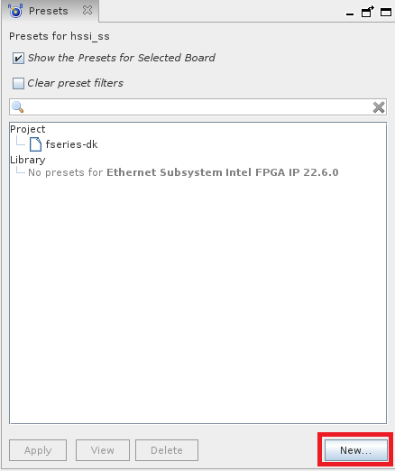
-
In the New Preset window, create a unique Name. In this example the name is
n6001-hssi-presets.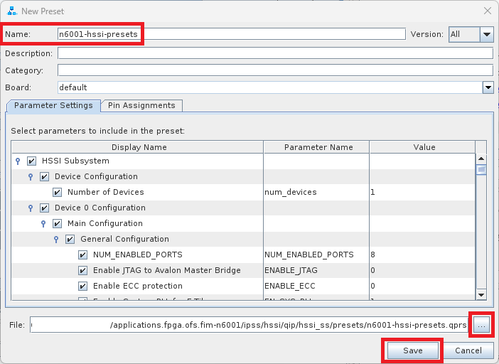
-
Click the ... button to select where to save the preset file. Give it a name, and save it to
$OFS_ROOTDIR/ipss/hssi/qip/hssi_ss/presets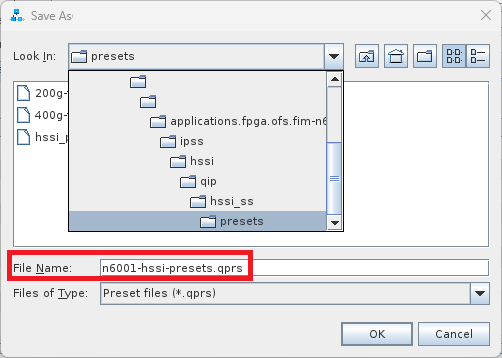
-
Click Save in the New Preset window. Click No when prompted to add the file to the IP search path.
-
Close out of all Quartus GUIs. You do not need to save or compile the IP.
-
Create a new HSSI OFSS file in the
$OFS_ROOTDIR/tools/ofss_config/hssidirectory namedhssi_preset_n6001.ofsswith the following contents. Note that thenum_channelsanddata_ratesettings will be overwritten by the contents of the preset file. Thepresetsetting must match the name you selected in Step 7. -
Edit the
$OFS_ROOTDIR/tools/ofss_config/n6001.ofssfile to use the new HSSI OFSS file created in Step 10. -
Compile the design using the n6001 OFSS file. It is recommended to compile a flat design first before incorporating a PR region in the design. This reduces design complexity while you modify the FIM.
-
The resulting FIM will contain the Ethernet-SS configuration specified by the presets file. The Ethernet-SS IP in the resulting work directory shows the parameter settings that are used.
4.8.4 Walkthrough: Modify the Ethernet Sub-System Without HSSI OFSS
This walkthrough describes how to modify the Ethernet-SS wihout using OFSS. This flow will edit the Ethernet-SS IP source directly. This walkthrough is useful for users who wish to make all Ethernet-SS modifications manually, without leveraging HSSI OFSS.
Pre-Requisites:
- This walkthrough requires a development environment. Refer to the Set Up Development Environment Section for instructions on setting up a development environment.
Steps:
-
Clone the OFS PCIe Attach FIM repository (or use an existing cloned repository). Refer to the Clone FIM Repository section for step-by-step instructions.
-
Set development environment variables. Refer to the Set Development Environment Variables section for step-by-step instructions.
-
Open the Ethernet-SS IP in Quartus Parameter Editor. Make your modifications in the Parameter Editor.
-
Once you are satisfied with your changes, click the Generate HDL. Save the design if prompted.
-
Compile the design.
-
If you are not using any other OFSS files in your compilation flow, use the following command to compile. It is recommended to compile a flat design before incorporating a PR region in the design. This reduces design complexity while you modify the FIM.
- If you are using OFSS files for other IP in the design, ensure that the top level OFSS file (e.g.
$OFS_ROOTDIR/tools/ofss_config/n6001.ofss) does not specify an HSSI OFSS file. Then use the following command to compile. It is recommended to compile a flat design first before incorporating a PR region in the design. This reduces design complexity while you modify the FIM.
-
-
The resulting FIM will contain the Ethernet-SS configuration contained in the
hssi_ss.ipsource file.
4.9 Modifying the HPS
This section describes ways to modify the HPS.
4.9.1 Walkthrough: Remove the HPS
Perform the following steps to remove the HPS from the FIM design.
Note: The n6000 default FIM has the HPS and Memory-SS disabled by default. This walkthrough targets the n6001.
Pre-requisites:
- This walkthrough requires a development environment. Refer to the Set Up Development Environment Section for instructions on setting up a development environment.
Steps:
-
Clone the OFS PCIe Attach FIM repository (or use an existing cloned repository). Refer to the Clone FIM Repository section for step-by-step instructions.
-
Set development environment variables. Refer to the Set Development Environment Variables section for step-by-step instructions.
-
Create a Memory Sub-system IP presets file with the connection to the HPS removed.
-
Open the the Memory Sub-System IP
-
In the IP Parameter Editor window that opens, remove the entries corresponding to the HPS (row #4) in the Memory Interfaces and Application Interfaces sections. To do this, click the row to be removed, then click the minus (
-) button.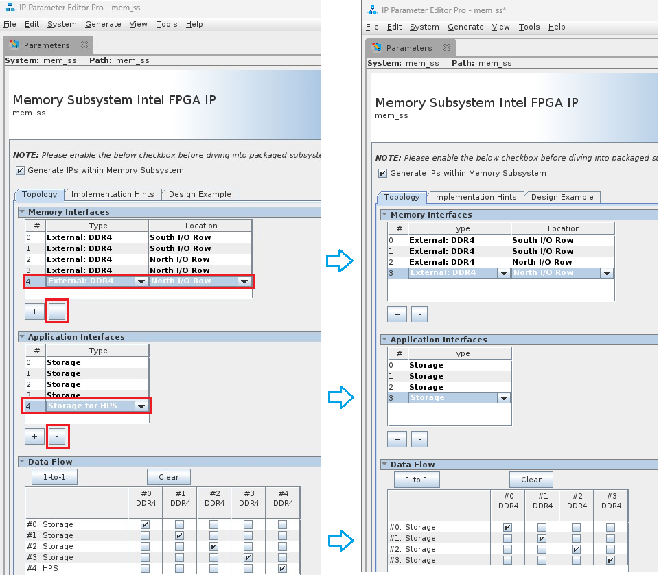
-
In the Presets pane, click New... to create a new IP presets file.
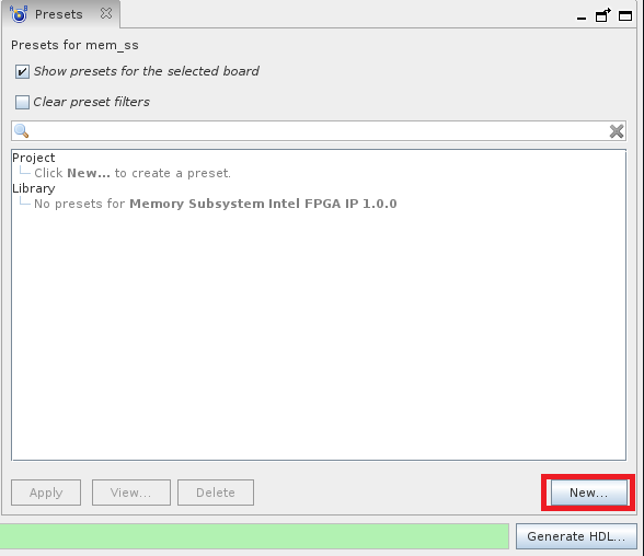
-
In the New Preset window, create a unique preset name. For example,
n6001-mem-no-hps.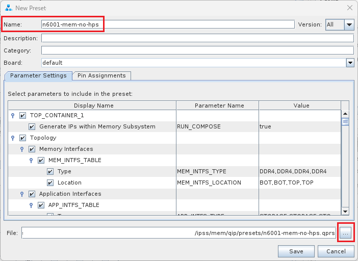
-
Click the ... button to select the save location of the IP presets file. In the Save As window, set the Look In field to the memory IP presets directory
$OFS_ROOTDIR/ipss/mem/qip/presets. Set the File Name field to match the name selected in Step 4. Click OK.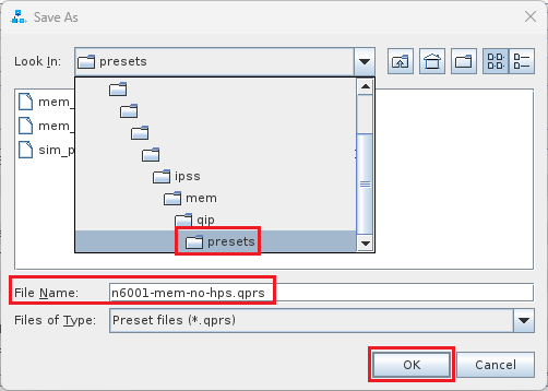
-
Click Save in the New Preset window. Click No when prompted to add the file to the IP search path.
-
Close IP Parameter Editor without saving or generating HDL.
-
-
Edit the Memory OFSS file
$OFS_ROOTDIR/tools/ofss_config/memory/memory.ofssto use the IP presets file generated in Step 4. -
Edit
$OFS_ROOTDIR/syn/board/n6001/syn_top/ofs_top.qsfto comment out theINCLUDE_HPSandINCLUDE_UARTmacro definitions. -
Build the FIM.
4.9.1 Walkthrough: Add the HPS
Note: The n6001 default FIM has the HPS and Memory-SS enabled by default. This walkthrough targets the n6000.
Pre-requisites:
- This walkthrough requires a development environment. Refer to the Set Up Development Environment Section for instructions on setting up a development environment.
Steps:
-
Clone the OFS PCIe Attach FIM repository (or use an existing cloned repository). Refer to the Clone FIM Repository section for step-by-step instructions.
-
Set development environment variables. Refer to the Set Development Environment Variables section for step-by-step instructions.
-
Edit
$OFS_ROOTDIR/syn/board/n6000/syn_top/ofs_top.qsfto un-comment theINCLUDE_DDR4,INCLUDE_HPS, andINCLUDE_UARTmacro definitions. -
Build the FIM.
5. FPGA Configuration
Configuring the Agilex FPGA on the n6001 can be done by Remote System Update (RSU) using OPAE commands, or by programming a SOF image to the FPGA via JTAG using Quartus Programer.
Programming via RSU will program the flash device on the board for non-volatile image updates. Programming via JTAG will configure the FPGA for volatile image updates.
5.1 Walkthrough: Set up JTAG
Perform the following steps to set up a JTAG connection to the Intel® FPGA SmartNIC N6001-PL.
Pre-requisites:
- This walkthrough requires an OFS Agilex PCIe Attach deployment environment. Refer to the Getting Started Guide: OFS for Agilex® 7 PCIe Attach FPGAs (Intel® FPGA SmartNIC N6001-PL/N6000-PL) for instructions on setting up a deployment environment.
- This walkthrough requires a workstation with Quartus Prime Pro Version 23.4 tools installed, specifically the
jtagconfigtool.
- This walkthrough requires an Intel FPGA Download Cable II.
Steps:
-
Set the board switches to dynamically select either the Agilex® 7 FPGA or MAX® 10 device on the JTAG chain.
- Set SW1.1=ON as shown in the next image. The switches are located at the back of the Intel® FPGA SmartNIC N6001-PL.
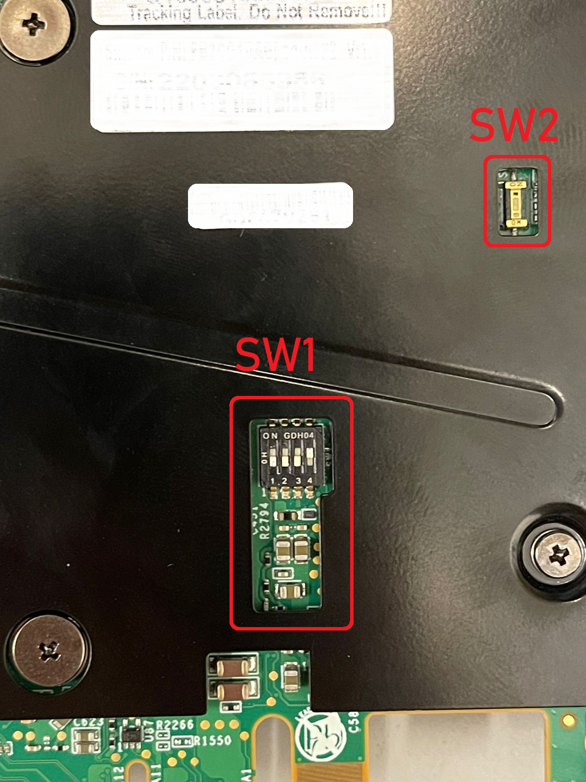
-
The Intel® FPGA SmartNIC N6001-PL has a 10 pin JTAG header on the top side of the board. Connect an Intel FPGA Download II Cable to the JTAG header of the Intel® FPGA SmartNIC N6001-PL as shown in picture below. This picture shows the Intel® FPGA SmartNIC N6001-PL card installed in the middle bay, top slot of a SuperMicro® SYS-220HE-FTNR server where the lower slot does not have card installed allowing the Intel® FPGA Download II cables to pass through removed the slot access.

Note: If using the Intel FGPA download Cable on Linux, add the udev rule as described in Intel FPGA Download Cable Driver for Linux.
-
Set the JTAG chain to select the Agilex® 7 FPGA as the target by writing to the JTAG enable register in the BMC (Register
0x378). This is done via PMCI registers0x2040Cand0x20400.Note: The commands below are targeted to a board with PCIe B:D.F of 98:00.0. Use the correct PCIe B:D.F of your card.
sudo opae.io init -d 0000:98:00.0 $USER
sudo opae.io -d 0000:98:00.0 -r 0 poke 0x2040c 0x100000000
sudo opae.io -d 0000:98:00.0 -r 0 poke 0x20400 0x37800000002
sudo opae.io release -d 0000:98:00.0
Note: To later re-direct the JTAG back to the MAX 10 device, execute the following commands.
sudo opae.io init -d 0000:b1:00.0 $USER
sudo opae.io -d 0000:b1:00.0 -r 0 poke 0x2040c 0x000000000
sudo opae.io -d 0000:b1:00.0 -r 0 poke 0x20400 0x37800000002
sudo opae.io release -d 0000:b1:00.0
Optionally, rather than dynamically commanding Agilex® 7 FPGA/MAX10 selection with the PMCI register settings, you can fix the selection with the following switch settings shown in the table below:
SW1.1 SW2 JTAG Target OFF OFF Agilex® 7 FPGA OFF ON MAX® 10 FPGA ON X Agilex® 7 FPGA if BMC register 0x378=0x1ON X MAX® 10 FPGA if BMC register 0x378=0x0 -
Use the
jtagconfigtool to check that the JTAG chain contains the AGFB014R24A2E2V device.
5.2 Walkthrough: Program the FPGA via JTAG
This walkthrough describes the steps to program the Agilex FPGA on the Intel® FPGA SmartNIC N6001-PL with a SOF image via JTAG.
Pre-Requisites:
- This walkthrough requires an OFS Agilex PCIe Attach deployment environment. Refer to the Getting Started Guide: OFS for Agilex® 7 PCIe Attach FPGAs (Intel® FPGA SmartNIC N6001-PL/N6000-PL) for instructions on setting up a deployment environment.
- This walkthrough requires a
SOFimage which will be programmed to the Agilex FPGA. Refer to the Compile OFS FIM Section for step-by-step instructions for generating aSOFimage.
- This walkthrough requires a JTAG connection to the n6001. Refer to the Set up JTAG section for step-by-step instructions.
- This walkthrough requires a Full Quartus Installation or Standalone Quartus Prime Programmer & Tools running on the machine where the Intel® FPGA SmartNIC N6001-PL is connected via JTAG.
Steps:
-
Start in your deployment environment.
-
If the card is already programmed with an OFS enabled design, determine the PCIe B:D.F of the card using OPAE command
fpgainfo fme. In this example, the PCIe B:D.F isB1:00.0.Example output:
Intel Acceleration Development Platform N6001 Board Management Controller NIOS FW version: 3.15.0 Board Management Controller Build version: 3.15.0 PBA: B#FB2CG1@AGF14-A0P2 MMID: 217000 SN: Q171211700050 //****** FME ******// Interface : DFL Object Id : 0xEF00000 PCIe s:b:d.f : 0000:98:00.0 Vendor Id : 0x8086 Device Id : 0xBCCE SubVendor Id : 0x8086 SubDevice Id : 0x1771 Socket Id : 0x00 Ports Num : 01 Bitstream Id : 360571653789875893 Bitstream Version : 5.0.1 Pr Interface Id : 5d4500ed-e5e5-5521-8865-e47f0c517fac Boot Page : user1 Factory Image Info : 9035190d637c383453173deb5de25fdd User1 Image Info : 893e691edfccfd0aecb1c332ad69551b User2 Image Info : 8cd2ae8073e194525bcd682f50935fc7 -
Remove the card from PCIe prior to programming. This will disable AER for the PCIe root port to prevent a surprise link-down event during programming.
-
Switch to the machine with JTAG connection to the n6001, if different than your deployment machine.
-
Open the Quartus programmer GUI
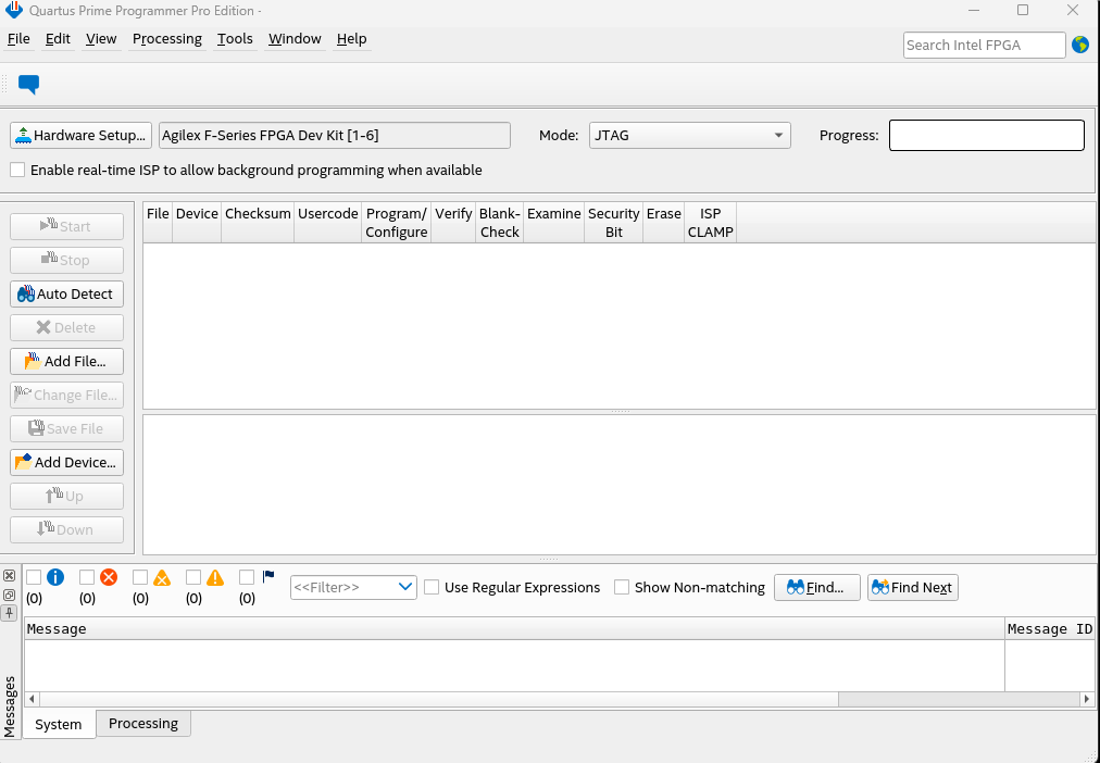
-
Click Hardware Setup to open the Hardware Setup dialog window.
-
In the Currently selected hardware field select the n6001.
-
In the Hardware frequency field enter
16000000Hz
-
Click Close
-
-
In the Quartus Prime Programmer window, click Auto Detect.
-
If prompted, select the AGFB014R24A2E2V device. The JTAG chain should show the divice.
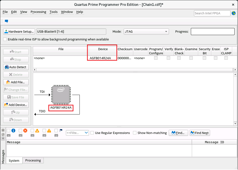
-
Right click the AGFB014R24A2E2V row and selct Change File.
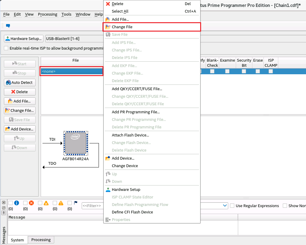
-
In the Select New Programming File window that opens, select the
.sofimage you wish to program and click Open. -
Check the Program/Configure box for the AGFB014R24A2E2V row, then click Start. Wait for the Progress bar to show
100% (Success). -
Close the Quartus Programmer GUI. You can answer 'No' if a dialog pops up asking to save the 'Chain.cdf' file
-
Switch to the deployment environment, if different than the JTAG connected machine.
-
Replug the board PCIe
-
Run
fpgainfo fmeto verify communication with the board, and to check the PR Interface ID.Intel Acceleration Development Platform N6001 Board Management Controller NIOS FW version: 3.15.0 Board Management Controller Build version: 3.15.0 PBA: B#FB2CG1@AGF14-A0P2 MMID: 217000 SN: Q171211700050 //****** FME ******// Interface : DFL Object Id : 0xEF00000 PCIe s:b:d.f : 0000:98:00.0 Vendor Id : 0x8086 Device Id : 0xBCCE SubVendor Id : 0x8086 SubDevice Id : 0x1771 Socket Id : 0x00 Ports Num : 01 Bitstream Id : 360571653789875893 Bitstream Version : 5.0.1 Pr Interface Id : 5d4500ed-e5e5-5521-8865-e47f0c517fac Boot Page : user1 Factory Image Info : 9035190d637c383453173deb5de25fdd User1 Image Info : 893e691edfccfd0aecb1c332ad69551b User2 Image Info : 8cd2ae8073e194525bcd682f50935fc7
5.3 Remote System Update
The OPAE fpgasupdate tool can be used to update the Max10 Board Management Controller (BMC) image and firmware (FW), root entry hash, and FPGA Static Region (SR) and user image (PR). The fpgasupdate tool only accepts images that have been formatted using PACsign. If a root entry hash has been programmed onto the board, then you must also sign the image using the correct keys. Refer to the Security User Guide: Open FPGA Stack for information on created signed images and on programming and managing the root entry hash.
The Intel® FPGA SmartNIC N6001-PL ships with a factory, user1, and user2 programmed image for both the FIM and BMC FW and RTL on all cards. The platform ships with a single FIM image that can be programmed into either user1 or user2, depending in the image selected.
5.3.1 Walkthrough: Program the FPGA via RSU
This walkthrough describes the steps to program the Agilex FPGA on the Intel® FPGA SmartNIC N6001-PL with a BIN image via RSU.
Pre-Requisites:
- This walkthrough requires an OFS Agilex PCIe Attach deployment environment. Refer to the Getting Started Guide: OFS for Agilex® 7 PCIe Attach FPGAs (Intel® FPGA SmartNIC N6001-PL/N6000-PL) for instructions on setting up a deployment environment.
- This walkthrough requires a
BINimage which will be programmed to the Agilex FPGA. Refer to the Compile OFS FIM Section for step-by-step instructions for generating aBINimage. The image used for programming must be formatted with PACsign before programming. This is done automatically by the build script.
Steps:
-
Start in your deployment environment.
-
Determine the PCIe B:D.F of the card using OPAE command
fpgainfo fme. In this example, the PCIe B:D.F isB1:00.0.Example output:
Intel Acceleration Development Platform N6001 Board Management Controller NIOS FW version: 3.15.0 Board Management Controller Build version: 3.15.0 PBA: B#FB2CG1@AGF14-A0P2 MMID: 217000 SN: Q171211700050 //****** FME ******// Interface : DFL Object Id : 0xEF00000 PCIe s:b:d.f : 0000:98:00.0 Vendor Id : 0x8086 Device Id : 0xBCCE SubVendor Id : 0x8086 SubDevice Id : 0x1771 Socket Id : 0x00 Ports Num : 01 Bitstream Id : 360571653789875893 Bitstream Version : 5.0.1 Pr Interface Id : 5d4500ed-e5e5-5521-8865-e47f0c517fac Boot Page : user1 Factory Image Info : 9035190d637c383453173deb5de25fdd User1 Image Info : 893e691edfccfd0aecb1c332ad69551b User2 Image Info : 8cd2ae8073e194525bcd682f50935fc7 -
Use the OPAE
fpgasupdatecommand to program a PACsign signed image to flash. The flash slot which will be programmed is determined by the PACsign header.-
Example: update User Image 1 in flash
-
Example: update User Image 2 in flash
-
Example: update Factory Image in flash
-
-
Use the OPAE
rsucommand to reconfigure the FPGA with the new image. You may select which image to configure from (User 1, User 2, Factory).-
Example: configure FPGA with User 1 Image
-
Example: configure FPGA with User 2 Image
-
Example: configure FPGA with Factory Image
-
Appendix
Appendix A: Resource Utilization Tables
Table A-1 Default Out-of-Tree FIM Resource Utilization
| Compilation Hierarchy Node | ALMs needed | ALM Utilization % | M20Ks | M20K Utilization % |
|---|---|---|---|---|
| top | 181,018.30 | 37.15 | 784 | 11.03 |
| afu_top | 104,994.20 | 21.55 | 287 | 4.04 |
| pcie_wrapper | 36,565.00 | 7.51 | 195 | 2.74 |
| hssi_wrapper | 20,132.10 | 4.13 | 173 | 2.43 |
| mem_ss_top | 9,092.80 | 1.87 | 76 | 1.07 |
| pmci_wrapper | 4,269.30 | 0.88 | 26 | 0.37 |
| alt_sld_fab_0 | 2,726.90 | 0.56 | 13 | 0.18 |
| bpf | 1,364.60 | 0.28 | 0 | 0.00 |
| qsfp_top | 620.10 | 0.13 | 4 | 0.06 |
| fme_top | 615.30 | 0.13 | 6 | 0.08 |
| qsfp_top | 614.00 | 0.13 | 4 | 0.06 |
| rst_ctrl | 17.90 | 0.00 | 0 | 0.00 |
| sys_pll | 0.50 | 0.00 | 0 | 0.00 |
| hps_ss | 0.00 | 0.00 | 0 | 0.00 |
Table A-2 Minimal FIM Resource Utilization
| Compilation Hierarchy Node | ALMs needed | ALM Utilization % | M20Ks | M20K Utilization % |
|---|---|---|---|---|
| 103192.5 | 21.18 | 410 | 5.77 | |
| afu_top | 45848.7 | 9.41 | 150 | 2.11 |
| auto_fab_0 | 1770.1 | 0.36 | 9 | 0.13 |
| bpf | 1265.8 | 0.26 | 0 | 0.0 |
| fme_top | 662.4 | 0.14 | 6 | 0.08 |
| hps_ss | 0.0 | 0.0 | 0 | 0.0 |
| hssi_dummy_csr | 675.5 | 0.14 | 0 | 0.0 |
| mem_ss_top | 8723.9 | 1.79 | 60 | 0.84 |
| pcie_wrapper | 38361.7 | 7.87 | 159 | 2.24 |
| pmci_wrapper | 4509.9 | 0.93 | 26 | 0.37 |
| qsfp0_dummy_csr | 672.2 | 0.14 | 0 | 0.0 |
| qsfp1_dummy_csr | 681.7 | 0.14 | 0 | 0.0 |
| rst_ctrl | 18.0 | 0.0 | 0 | 0.0 |
| sys_pll | 0.5 | 0.0 | 0 | 0.0 |
Appendix B: Glossary
| Term | Abbreviation | Description |
|---|---|---|
| Advanced Error Reporting | AER | The PCIe AER driver is the extended PCI Express error reporting capability providing more robust error reporting. (link) |
| Accelerator Functional Unit | AFU | Hardware Accelerator implemented in FPGA logic which offloads a computational operation for an application from the CPU to improve performance. Note: An AFU region is the part of the design where an AFU may reside. This AFU may or may not be a partial reconfiguration region. |
| Basic Building Block | BBB | Features within an AFU or part of an FPGA interface that can be reused across designs. These building blocks do not have stringent interface requirements like the FIM's AFU and host interface requires. All BBBs must have a (globally unique identifier) GUID. |
| Best Known Configuration | BKC | The software and hardware configuration Intel uses to verify the solution. |
| Board Management Controller | BMC | Supports features such as board power managment, flash management, configuration management, and board telemetry monitoring and protection. The majority of the BMC logic is in a separate component, such as an Intel® Max® 10 or Intel Cyclone® 10 device; a small portion of the BMC known as the PMCI resides in the main Agilex FPGA. |
| Configuration and Status Register | CSR | The generic name for a register space which is accessed in order to interface with the module it resides in (e.g. AFU, BMC, various sub-systems and modules). |
| Data Parallel C++ | DPC++ | DPC++ is Intel’s implementation of the SYCL standard. It supports additional attributes and language extensions which ensure DCP++ (SYCL) is efficiently implanted on Intel hardware. |
| Device Feature List | DFL | The DFL, which is implemented in RTL, consists of a self-describing data structure in PCI BAR space that allows the DFL driver to automatically load the drivers required for a given FPGA configuration. This concept is the foundation for the OFS software framework. (link) |
| FPGA Interface Manager | FIM | Provides platform management, functionality, clocks, resets and standard interfaces to host and AFUs. The FIM resides in the static region of the FPGA and contains the FPGA Management Engine (FME) and I/O ring. |
| FPGA Management Engine | FME | Performs reconfiguration and other FPGA management functions. Each FPGA device only has one FME which is accessed through PF0. |
| Host Exerciser Module | HEM | Host exercisers are used to exercise and characterize the various host-FPGA interactions, including Memory Mapped Input/Output (MMIO), data transfer from host to FPGA, PR, host to FPGA memory, etc. |
| Input/Output Control | IOCTL | System calls used to manipulate underlying device parameters of special files. |
| Intel Virtualization Technology for Directed I/O | Intel VT-d | Extension of the VT-x and VT-I processor virtualization technologies which adds new support for I/O device virtualization. |
| Joint Test Action Group | JTAG | Refers to the IEEE 1149.1 JTAG standard; Another FPGA configuration methodology. |
| Memory Mapped Input/Output | MMIO | The memory space users may map and access both control registers and system memory buffers with accelerators. |
| oneAPI Accelerator Support Package | oneAPI-asp | A collection of hardware and software components that enable oneAPI kernel to communicate with oneAPI runtime and OFS shell components. oneAPI ASP hardware components and oneAPI kernel form the AFU region of a oneAPI system in OFS. |
| Open FPGA Stack | OFS | OFS is a software and hardware infrastructure providing an efficient approach to develop a custom FPGA-based platform or workload using an Intel, 3rd party, or custom board. |
| Open Programmable Acceleration Engine Software Development Kit | OPAE SDK | The OPAE SDK is a software framework for managing and accessing programmable accelerators (FPGAs). It consists of a collection of libraries and tools to facilitate the development of software applications and accelerators. The OPAE SDK resides exclusively in user-space. |
| Platform Interface Manager | PIM | An interface manager that comprises two components: a configurable platform specific interface for board developers and a collection of shims that AFU developers can use to handle clock crossing, response sorting, buffering and different protocols. |
| Platform Management Controller Interface | PMCI | The portion of the BMC that resides in the Agilex FPGA and allows the FPGA to communicate with the primary BMC component on the board. |
| Partial Reconfiguration | PR | The ability to dynamically reconfigure a portion of an FPGA while the remaining FPGA design continues to function. For OFS designs, the PR region is referred to as the pr_slot. |
| Port | N/A | When used in the context of the fpgainfo port command it represents the interfaces between the static FPGA fabric and the PR region containing the AFU. |
| Remote System Update | RSU | The process by which the host can remotely update images stored in flash through PCIe. This is done with the OPAE software command "fpgasupdate". |
| Secure Device Manager | SDM | The SDM is the point of entry to the FPGA for JTAG commands and interfaces, as well as for device configuration data (from flash, SD card, or through PCI Express* hard IP). |
| Static Region | SR | The portion of the FPGA design that cannot be dynamically reconfigured during run-time. |
| Single-Root Input-Output Virtualization | SR-IOV | Allows the isolation of PCI Express resources for manageability and performance. |
| SYCL | SYCL | SYCL (pronounced "sickle") is a royalty-free, cross-platform abstraction layer that enables code for heterogeneous and offload processors to be written using modern ISO C++ (at least C++ 17). It provides several features that make it well-suited for programming heterogeneous systems, allowing the same code to be used for CPUs, GPUs, FPGAs or any other hardware accelerator. SYCL was developed by the Khronos Group, a non-profit organization that develops open standards (including OpenCL) for graphics, compute, vision, and multimedia. SYCL is being used by a growing number of developers in a variety of industries, including automotive, aerospace, and consumer electronics. |
| Test Bench | TB | Testbench or Verification Environment is used to check the functional correctness of the Design Under Test (DUT) by generating and driving a predefined input sequence to a design, capturing the design output and comparing with-respect-to expected output. |
| Universal Verification Methodology | UVM | A modular, reusable, and scalable testbench structure via an API framework. In the context of OFS, the UVM enviroment provides a system level simulation environment for your design. |
| Virtual Function Input/Output | VFIO | An Input-Output Memory Management Unit (IOMMU)/device agnostic framework for exposing direct device access to userspace. (link) |
Notices & Disclaimers
Intel® technologies may require enabled hardware, software or service activation. No product or component can be absolutely secure. Performance varies by use, configuration and other factors. Your costs and results may vary. You may not use or facilitate the use of this document in connection with any infringement or other legal analysis concerning Intel products described herein. You agree to grant Intel a non-exclusive, royalty-free license to any patent claim thereafter drafted which includes subject matter disclosed herein. No license (express or implied, by estoppel or otherwise) to any intellectual property rights is granted by this document, with the sole exception that you may publish an unmodified copy. You may create software implementations based on this document and in compliance with the foregoing that are intended to execute on the Intel product(s) referenced in this document. No rights are granted to create modifications or derivatives of this document. The products described may contain design defects or errors known as errata which may cause the product to deviate from published specifications. Current characterized errata are available on request. Intel disclaims all express and implied warranties, including without limitation, the implied warranties of merchantability, fitness for a particular purpose, and non-infringement, as well as any warranty arising from course of performance, course of dealing, or usage in trade. You are responsible for safety of the overall system, including compliance with applicable safety-related requirements or standards. © Intel Corporation. Intel, the Intel logo, and other Intel marks are trademarks of Intel Corporation or its subsidiaries. Other names and brands may be claimed as the property of others.
OpenCL and the OpenCL logo are trademarks of Apple Inc. used by permission of the Khronos Group™.